


- News
11 May 2017
Fraunhofer IAF develops first monolithically integrated half-bridge for 600V-class
Fraunhofer Institute for Applied Solid State Physics (IAF) of Freiburg, Germany has developed what is claimed to be the first half-bridge circuit for the important 600V class in which all the electronic components are monolithically integrated on one chip. Monolithically integrated half bridges are key building blocks of compact voltage converters and significantly increase the efficiency of power electronics devices.
Used in mains adapters and chargers for smartphones, laptops and low-voltage household appliances, voltage converters are in increasingly widespread demand as more and more electrical devices are being plugged into mains power supplies. The energy transition and e-mobility are also increasing the demand for reliable and, above all, efficient and compact voltage converters of all kinds. Half-bridge circuits are the centerpiece of many voltage converters.
In power electronics components, 600V is the standard volt class for grid-connected electrical devices, ranging from tablets and washing machines to e-bikes and electric cars.
Besides being very compact, monolithically integrated half-bridge circuits have much better electronic properties, e.g. the switching frequency can be improved by a factor of about 10 compared with conventional voltage converters. “A switching frequency of up to 3MHz allows us to achieve a much greater power density. This is very important in areas such as e-mobility, where many converters which are as efficient as possible have to be fitted in very little space,” says Richard Reiner, research associate in Fraunhofer IAF’s Power Electronics business unit. Monolithically integrated half-bridges are more compact, are easier to assemble and improve reliability.
High-performance on-board chargers for electric cars
The German government has set itself the target of putting 1 million electric cars on the country’s roads by 2020. Covering long distances without generating any emissions requires not only powerful batteries but also the development of lightweight electric cars that generate as little energy as possible. This can only be accomplished using electronic components based on materials such as gallium nitride (GaN), which in contrast to silicon carbide (SiC) can be grown as an epitaxial layer on cost-effective, large-area silicon substrates. When used in electronic components for electric vehicles, GaN enables higher power densities to be achieved more energy efficiently. The aim of car makers and users is to develop extremely efficient on-board chargers for electric vehicles that take up as little space as possible.
Their compact design minimizes negative influences such as line impedances, improving the electrical switching characteristics. The integration of additional sensor technology, such as a thermal monitoring system, improves operation even further. “This innovative approach brings a new level of power density, efficiency, robustness, functionality and reliability to e-mobility,” says Dr Patrick Waltereit, deputy head of Fraunhofer IAF’s Power Electronics business unit.
Design of monolithically integrated half-bridge circuit
Fraunhofer IAF’s half-bridge circuit comprises two GaN high-electron-mobility transistors (HEMTs) and two integrated freewheeling diodes. The HEMTs have a breakdown voltage of more than 600V and an on-state resistance of 120mΩ. A folded chip layout enables the DC link capacitance to be tightly connected between the supply voltage and ground. This design creates an optimized power path and allows clean, stable switching at high frequencies. Operation of this circuit was demonstrated at the 4th IEEE Workshop on Wide Bandgap Power Devices and Applications (WiPDA 2016) in Fayetteville, AR, USA last November in a down-converter from 400V to 200V at a switching frequency of 3MHz.
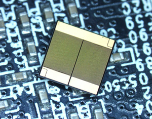 Picture: Fraunhofer IAF’s monolithically integrated half-bridge circuit. © Photo Fraunhofer IAF
Even more complex circuits, such as a monolithically integrated multi-level inverter, have already been produced using this GaN-on-Si technology. In this topology, ten GaN power devices are placed on one chip with an area of 2mm x 3mm. Each switch has a breakdown voltage of 400V in the off state and a resistance of 350mΩ in the on state. Compared with conventional converters, multi-level inverters generate less noise during DC/AC conversion. This means that they require smaller output filters. Monolithic integration therefore not only reduces costs, but also makes voltage converters more compact and lightweight. This converter was demonstrated in inverters operating at the mains voltage level used in the USA (120V).
Fraunhofer IAF is presenting its monolithically integrated half-bridge circuit in booth 237 (hall 7) at the PCIM (Power Conversion Intelligent Motion) Europe 2017 trade show in Nuremberg, Germany (16-18 May).
IAF GaN-on-Si GaN HEMT Power electronics
www.mesago.de/en/PCIM/main.htm


