


- News
6 November 2017
Kyma demos 200mm GaN HVPE on QROMIS’ MOCVD GaN-on-QST wafers
© Semiconductor Today Magazine / Juno Publishing
Kyma Technologies Inc of Raleigh, NC, USA - which provides wide-bandgap semiconductor crystalline materials, crystal growth equipment, and GaN-based photoconductive semiconductor switch (PCSS) devices - has used its new K200 hydride vapor phase epitaxy (HVPE) growth tool to produce high-quality 200mm-diameter HVPE GaN-on-QST (QROMIS Substrate Technology) templates.
This follows Kyma’s demonstration in 2016 of 150mm-diameter GaN-on-QST templates in partnership with QROMIS Inc of Santa Clara, CA, USA (formerly Quora Technology Inc, spun off from Micron Technology in March 2015) and Kyma’s commissioning of its K200 HVPE growth tool in June 2017.
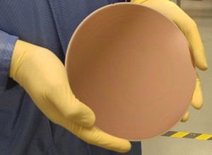 Picture: A 200mm-diameter HVPE GaN-on-QST template.
The demonstrated 200mm-diameter HVPE GaN-on-QST template consists of 10μm of HVPE gallium nitride (GaN) grown on a 5μm metal-organic chemical vapor deposition (MOCVD) GaN-on-QST wafer provided by QROMIS. X-ray diffraction (XRD) rocking curve linewidths for the templates fall in the range 250-330arc-sec for the symmetric {002) and asymmetric {102} XRD peaks, respectively, which is consistent with high structural quality. Low wafer bow (~50μm) and smooth surface morphology suggest that these materials should support high-performance device manufacturing.
Kyma says that its newly constructed K200 HVPE tool represents a first for the industry and was designed to enable uniform and rapid growth of high-quality GaN on a number of different substrates.
“We have successfully transferred the process for making high-quality GaN to our K200 HVPE tool,” notes president & CEO Keith Evans. “We are currently engaging with customers interested in large-diameter GaN-on-QST templates.”
Kyma and Qromis are partnered for this work under a Kyma-led US Department of Energy (DOE) Phase IIB Small Business Innovation Research (SBIR) award (number DE-SC0009653).
Fabless firm QROMIS recently began manufacturing 200mm QST substrates and GaN-on-QST wafers using its foundry partner Vanguard International Semiconductor (VIS), which is planning to offer GaN power device manufacturing services on 8-inch diameter QST platform in 2018.
“QROMIS’ CMOS-fab-friendly 200mm-diameter QST substrates and GaN-on-QST wafers represent a disruptive technology, enabling GaN epitaxy from a few microns to hundreds of microns for GaN power applications from 100V to 1500V-or-beyond GaN power devices, in lateral, quasi-vertical or vertical forms, on the same 8-inch or 12-inch production platform at silicon power device cost,” says QROMIS co-founder & CEO Cem Basceri. “Kyma’s K200 HVPE technology represents an important value-add to QST-based GaN power device manufacturing by enabling the low-cost deposition of a thicker and lower-defect-density GaN surface than is practically achievable using MOCVD growth alone.”
Kyma is also teamed with a semiconductor equipment OEM to manufacture K200 HVPE tools for customers who prefer to bring Kyma’s HVPE GaN growth process in-house.
Kyma and Quora partner on GaN substrate materials


