


- News
1 November 2017
III-nitride on silicon optoelectronics transfer to plastic and glass
Nanjing University of Posts and Telecommunications and Zhengzhou University in China have used gallium nitride (GaN) on silicon technology to fabricate light-emitting and light-detecting diodes that can be transferred to metal, plastic and glass substrates [Zheng Shi et al, Optical Materials, vol72, p20, 2017].
The epitaxial structures were grown by metal-organic chemical vapor phase deposition (MOCVD) on (111) silicon. Step-graded aluminium gallium nitride (AlGaN) was used as a buffer, bridging the thermal expansion and lattice mismatch between Si and GaN. Further layers consisted of a 3400nm n-GaN contact, nine 3nm indium gallium nitride (InGaN) multiple quantum wells (MQWs) separated by 10nm GaN barriers, and a 115nm p-GaN contact.
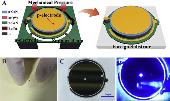
Figure 1: (A) Schematic fabrication and transfer procedures for MQW-diode-on-silicon. (B) Transferred MQW-diode on PET substrate. (C) Transferred MQW-diode on glass substrate. (D) Light emission image of MQW-diode-on-glass under current injection.
Circular 1.5mm-diameter diodes were fabricated with the nickel/gold p-electrode also serving as a reflector. The device was designed so that light entered or left through the back-side n-GaN. For transfer to foreign substrates, the back-side silicon, buffer and some of the n-GaN was etched with inductively coupled plasma, leaving the 2μm-thick diodes held in place with thin support beams (Figure 1). These struts were mechanically broken with probes for direct transfer to polyethylene terephthalate (PET) or glass substrates.
The flexibility of PET suggests the potential for adjustable displays and wearable optical sensors. The researchers see the GaN-based diodes as offering improved efficiency, reliability and long-term stability, compared with organic light-emitting devices.
Before transfer, the etched diodes emitted wavelengths that red-shifted from 453.7nm to 454.9nm wavelength as the injection current increased from 5mA to 50mA. On glass, the corresponding wavelengths were 455.8nm to 461.9nm. The red-shift on transfer to glass is attributed to optically induced charge carriers giving rise to an internal electric field. A further effect is distortion from self-heating, which is constrained before transfer. The researchers suggest that transfer to metal could help reduce self-heating effects.
The devices were also tested under 3Mbits per second pseudo-random modulation, suggesting the potential for light communications.
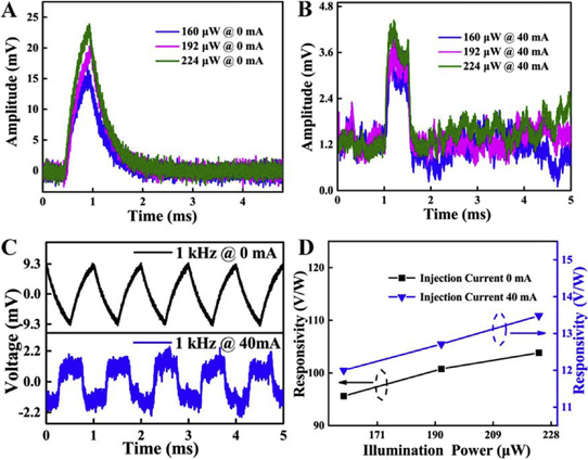
Figure 2: (A) Single light-detecting behavior of MQW-diode-on-glass. (B) Simultaneous light-detecting light-emitting behavior of MQW-diode-on-glass. (C) Continuously light-detecting response of MQW-diode-on-glass. (D) Induced voltage as a function of incident light power for MQW-diode-on-glass.
At zero current injection, the diodes responded to illumination pulses, rising to a peak and decaying. The researchers comment: “The 1.5mm-diameter MQW-diodes can be used as flexible solar cells to harvest energy from ambient light sources by integrating a capacitor circuit.”
The diode responded with sharper decay, giving a more pulse-like voltage change, when operated in dual-mode with 40mA current injection. “The light-detecting plots exhibit the sharp decay processes because the photo-generated electron-hole pairs are quickly canceled by the injected electrons and holes,” the team explains.
The dual-mode opens the possibility of full-duplex visible light communication. The millimeter-order size of the device could allow the integration of transmitter, waveguide, modulator and receiver functionality on a single chip.
Under 410nm wavelength illumination, the response at zero injection was ~100V/W. Dual-mode response with 40mA injection was ~10V/W.
InGaN AlGaN GaN GaN on silicon Light emitting diode Light detecting diode Glass substrates Plastic substrates MOCVD
http://dx.doi.org/10.1016/j.optmat.2017.05.039
The author Mike Cooke is a freelance technology journalist who has worked in the semiconductor and advanced technology sectors since 1997.


