


- News
20 October 2017
Vertical gallium nitride Schottky diodes with single and double drift layers
Arizona State University in the USA claims record low turn-on voltage, less than 0.6V, for its latest vertical gallium nitride on gallium nitride (GaN) Schottky barriers diodes (SBDs) [Houqiang Fu et al, Appl. Phys. Lett., vol111, p152102, 2017]. The researchers also developed a double drift layer to increase the breakdown voltage.
Vertical devices have recently been developed on free-standing or bulk GaN substrates for power applications. The use of free-standing/bulk substrates avoids generating high threading dislocation densities (more than 109/cm2 on sapphire) that provide unwanted leakage paths, reducing breakdown voltages.
The fabrication of Schottky rather than pn diodes allows the turn-on voltage to be reduced significantly below the bandgap. The large ~3V turn-on of pn diodes leads to large power losses in switching applications. However, Schottky diodes continue to have lower breakdown voltages and higher on-resistance than pn devices. Improving breakdown with thicker drift layers tends to increase on-resistance.
The researchers used n+-GaN bulk substrates from Sumitomo Electric Industries Ltd for metal-organic chemical vapor deposition (MOCVD) of the SBD materials (Figure 1). A conventional single drift layer diode, A, was compared with a double drift layer structure, B. Simulations suggested that diode B should be able to support much higher reverse biasing for the same peak electric field at the metal/semiconductor interface.
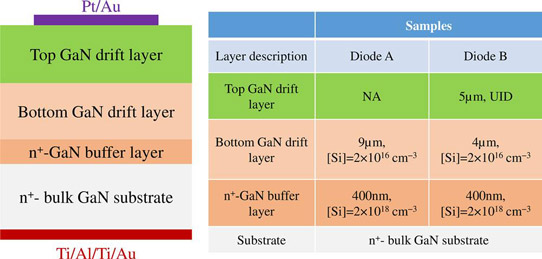
Figure 1: Schematic of cross section of GaN SBDs (left) and detailed descriptions of layers (right) for diode A and diode B.
Using x-ray analysis, the researchers estimated that the dislocation densities were in the low 106/cm2 range in both samples - “significantly lower than that of typical GaN devices grown on sapphire (>109/cm2),” they add.
Fabrication involved cleaning, inductively coupled plasma mesa etch, and the deposition of Schottky platinum/gold (Pt/Au) and ohmic titanium/aluminium/titanium/gold (Ti/Al/Ti/Au) ohmic contacts. There was no passivation, field plate (FP) or edge termination.
The turn-on voltages were 0.52V and 0.59V for diodes A and B, respectively. This gave corresponding forward voltages for 0.1mA current flow of 1.0V and 1.2V. The turn-on voltages are described as record lows for vertical GaN-on-GaN diodes. The diode B had an ideality factor of 1.04, compared with 1.06 for diode A. These values are described as nearly ideal (i.e. unity factor) for GaN SBDs.
The off-current density, the measurement of which was hampered by the 0.1nA lower limit of the test equipment, was below 10-7A/cm2 for both diodes. The on/off current ratio was about 1010, “among the highest values demonstrated in vertical GaN power diodes,” according to the team.
The on-resistance at 0.1A current was 1.39mΩ-cm2 for diode A and 1.65mΩ-cm2 for diode B. The slightly higher on-resistance of diode B is attributed to a lack of electrons in the top undoped drift layer. Subtracting out the effect of the substrate, the researchers estimate the drift-layer mobility at 886.1cm2/V-s and 1045.2cm2/V-s for diodes A and B, respectively. The team comments: “Diode A had a lower electron mobility, possibly due to stronger impurity scattering from silicon dopants.”
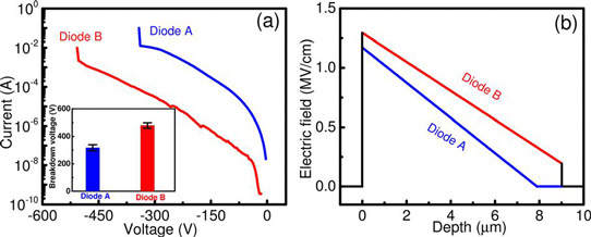
Figure 2: Reverse current-voltage characteristics of diodes A and B. Inset: measured breakdown voltages. (b) Electric field profiles along vertical direction of diodes.
The reverse-bias breakdowns for diodes A and B were, respectively, 340V and 503V (Figure 2). These values gave critical fields (1.17MV/cm and 1.30MV/cm, respectively) that were somewhat lower than expected values based on the critical field of GaN (~3.0MV/cm). The team reports: “Since we did not employ FP or edge termination, the breakdown was expected to be determined by the device edge breakdown. Optical microscopy examination confirmed that the catastrophic damages of the GaN SBDs indeed occurred at the edge of Schottky contacts possibly due to severe edge electric field crowding.”
Varying the temperature allowed extraction of the Schottky barrier heights (φB): 0.69eV for diode A and 0.70eV for B. The team comments; “The low φB values are partly responsible for the obtained record-low VON in forward bias. The measured φB values are less than the theoretical values, which demands further investigations. Possible explanations include surface roughness, non-uniform current distribution, and so on.”
GaN Schottky barriers diodes GaN substrate MOCVD
https://doi.org/10.1063/1.4993201
The author Mike Cooke is a freelance technology journalist who has worked in the semiconductor and advanced technology sectors since 1997.


