


- News
4 October 2017
Chicago and Cornell co-develop layer-by-layer assembly of 2D materials into wafer-scale heterostructures
Researchers at University of Chicago and Cornell University have reported an innovative method for making stacks of semiconductor layers just a few atoms thick (‘Layer-by-layer assembly of two-dimensional materials into wafer-scale heterostructures’, Kang et al, Nature (20 September), doi: 10.1038/nature23905). The technique is said to offer a simple, cost-effective method to make thin, uniform layers of these materials, which could expand capabilities for devices from solar cells to cell phones.
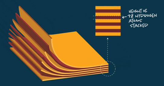
Picture: New method allows individual films, each just a few atoms high, to be fabricated and stacked.
Stacking thin layers of materials offers a range of possibilities for making electronic devices with unique properties, but manufacturing such films is a delicate process with little room for error, say the researchers.
“Imagine trying to lay down a flat sheet of plastic wrap the size of Chicago without getting any air bubbles in it,” says Jiwoong Park, a UChicago professor in the Department of Chemistry, the Institute for Molecular Engineering and the James Franck Institute, who led the study. “When the material itself is just atoms thick, every little stray atom is a problem,” he adds.
Currently, these layers are grown instead of stacking them on top of each other, but that means that the bottom layers must be subjected to harsh growth conditions such as high temperatures while the new ones are added — a process that limits the materials with which to make them.
Park’s team instead made the films individually. They then put them into a vacuum, peeled them off and stuck them to each other. This allowed the researchers to make films that were connected with weak (van der Waals) bonds instead of stronger covalent bonds — interfering less with the perfect surfaces between the layers.
“The films — vertically controlled at the atomic level — are exceptionally high quality over entire wafers,” says Kibum Kang, a postdoctoral associate who was the first author of the study.
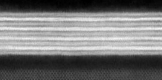
Picture: A stack of films (each just a few atoms thick), shown in cross-section using an electron microscope.
Kan-Heng Lee, a graduate student and co-first author of the study, then tested the films’ electrical properties by making them into devices and showed that their functions can be designed on the atomic scale, which could allow them to serve as the essential ingredient for future computer chips.
The researchers say that the method opens up a myriad of possibilities for such films. They can be made on top of water or plastics; they can be made to detach by dipping them into water; and they can be patterned with an ion beam. The team is exploring the full range of what can be done with the method, which they say is simple and cost-effective.
“We expect this new method to accelerate the discovery of novel materials, as well as enabling large-scale manufacturing,” Park says.
Funding for the research came from the US Air Force, National Science Foundation (NSF) and the National Research Foundation of Korea. It used the Materials Research Science and Engineering Centers (MRSEC) Shared User Facilities at UChicago and Cornell and the Pritzker Nanofabrication Facility at UChicago’s Institute for Molecular Engineering.
www.nature.com/nature/journal/vaop/ncurrent/full/nature23905.html


