


- News
10 October 2017
LayTec ships further EpiTT VCSEL systems to leading VCSEL maker in USA
Last year in-situ metrology system maker LayTec AG of Berlin, Germany reported the first sale of its EpiTT VCSEL (vertical-cavity surface-emitting laser) for indium phosphide (InP)-based epitaxy to a leading European customer. In second-quarter 2017 LayTec completed development of the respective tool for gallium arsenide (GaAs)-based VCSEL growth. The next two systems have now been shipped (in September) to a leading VCSEL maker in the USA.
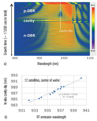
Picture: 940nm VCSEL grown in 12 x 4”-wafer Aixtron planetary G3 MOCVD reactor of a European industrial customer (full load qualification run). (a) shows the color-coded spectral fingerprint of satellite #1 (center of wafer). 36 such in-situ signatures have been generated for center/half-radius/edge regions of all the 12 wafers. (b) Room-temperature ex-situ on-wafer emission in the 12 wafer centers compared with the respective in-situ cavity dip wavelength position. The cavity dip measured in-situ is fitted automatically in real-time to the measured spectrum (after last AlGaAs layer of p-DBR was completed at growth-temperature) by LayTec’s EpiNet 2018 software. Extremely good correlation between in-situ measurement and ex-situ data demonstrates that EpiTT VCSEL gives a reliable forecast of device performance.
EpiTT VCSEL adds full spectral capabilities to the established performance of EpiTT (wafer temperature sensing at 950nm and growth rate measurement based on three-wavelength reflectance). Two spectral ranges can be chosen: 630-1100nm for GaAs-based near-infrared (NIR) VCSEL epitaxy and 1000-1700nm for InP-based IR VCSEL processes.
Either system delivers direct access to cavity dip position and stop-band wavelength control already during MOCVD. The cavity dip position is extremely sensitive to the accurate thickness and composition of QWs (quantum wells)/QBs (quantum barriers), oxidizing AlAs and other functional layers in the cavity. For optimum laser performance, this cavity dip position has to be in exact correlation to QW emission wavelength.
Here another strength of the EpiTT VCSEL comes into play: tight control of wafer temperature for highly precise QW composition. However, during cavity growth for some VCSEL designs, the standard wavelength of the pyrometer overlaps with the high-reflectivity band of the underlying n-doped distributed Bragg reflector (n-DBR), causing high reflectance and hence low thermal emissivity of the wafer. LayTec therefore added the possibility to customize the pyrometer wavelength of the EpiTT VCSEL.
A second pyrometer module can be chosen between 810nm, 850nm, 980nm. This allows accurate wafer temperature measurement for a wide range of VCSEL MOCVD processes. The Figure gives an example for a VCSEL with a target emission wavelength of 940nm.
LayTec receives first order for EpiTT/VCSEL


