


- News
4 October 2017
Reducing costs for gallium arsenide Schottky diode fabrication
The University of Sherbrooke and École de Technologie Supérieure in Canada have developed a gallium arsenide (GaAs) Schottky diode fabrication technique aimed at low-cost sub-millimeter wave performance [Sarvenaz Jenabi et al, Semicond. Sci. Technol., vol32, p105006, 2017]. The researchers used photolithography rather than the more expensive electron-beam patterning that is often used. Also, the number of metallization steps was reduced from five to two, reducing lithography alignment complexities from eight steps to five.
The team points out that, while Schottky diodes are key elements in electronic circuits, their fabrication becomes more and more challenging at high frequencies due to the small size of the device and high sensitivity to parasitic elements.
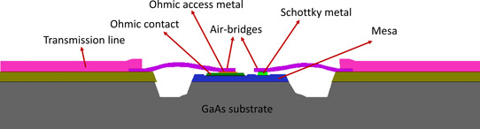
Figure 1: Schematic side view of fabricated diode.
A significant reduction in parasitic capacitance was achieved by the use of air-bridge connections to the transmission lines (Figure 1). The researchers report: “The proposed fabrication method with large stand-off height for the air-bridge, wide and deep trenches has reduced the parasitic capacitance to less than 0.7fF. We expect a practical cut-off frequency of 0.85 and 1.4THz for these diodes.”
The researchers used a GaAs wafer designed for heterojunction bipolar transistors, etching away unwanted layers to leave a lightly doped n-GaAs layer for the Schottky contact and a heavily doped n-GaAs ohmic contact region. The ohmic contact layer was 350nm thick.
The multi-step metallization (multi-SM) used wet mesa etching, germanium/gold/nickel/gold ohmic contact evaporation, rapid thermal anneal, and titanium/gold Schottky contact evaporation. The height of the ohmic contact was raised to that of the Schottky contact by depositing titanium/gold.
Air-bridge formation began with titanium/gold evaporation and deep trench etching around the mesa. The trench was filled with resist that was etched back with oxygen plasma until the air-bridge contact features appeared. Further deposition and patterning formed the titanium/gold air-bridge wiring and transmission lines, where the resist materials were removed in the lift-off process.
The researchers simplified this process into a ‘double-step’ process by combining the Schottky contact, air-bridge, and transmission-line metallization into a single step. This needed the deep trench to be created before the Schottky metal deposition. Also, the trench filling material was changed so that it consisted of two resist types: a ‘filling resist’ and a ‘cover resist’. The filling resist was chosen such that it was not affected by the cover resist developer. The filling resist also had a higher temperature tolerance.
The fill consisted of poly(methyl methacrylate) (PMMA) deposited in several layers. The lower part of the fill used low-concentration PMMA solution. The PMMA concentration was gradually increased for subsequent layers.
The thick cover resist was then spun onto the structure and patterned so that after development the cover resist was only found over the trench. The oxygen plasma etch rate for the cover resist was less than that of the PMMA so the final structure made an arch shape of resist over the trench. The non-trench surfaces were free of resist.
The researchers comment: “Unlike the multi-SM, this process is much less sensitive on the etching stop point since another resist will be spun over to form and support the air bridges and T-shaped anode.”
The T-shaped anode and air-bridge wiring was patterned through deep-ultraviolet lithography on a three-layer resist for metal lift-off processing. The bottom layer was poly-methyl-glutar-imide (PMGI). The top layer was from Shipley. The middle ‘undercut’ layer was chosen so that its developer would not affect the bottom PMGI layer. The PMGI layer enabled the formation of the tall-neck T-shaped anode. The titanium/gold metal was deposited after cleaning and passivation. The lift-off process then gives the Schottky contact (anode), air bridges, and transmission-line circuitry.
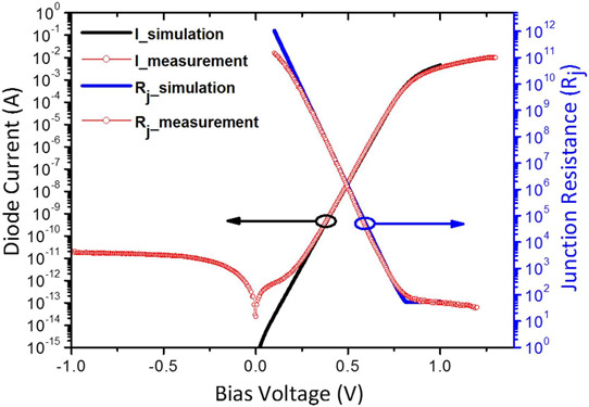
Figure 2: Simulated and measured current versus voltage bias of diode (left axis), and junction resistance versus voltage bias (right axis) for 1.5μm anode radius.
The capacitance of diodes with 1.5μm- and 1μm-diameter anodes were extracted as 7.1fF and 3.3fF, respectively. These values were based on S-parameter measurements between 2GHz and 40GHz. DC measurements (Figure 2) gave 5x10-16A saturation current, 1.13 ideality, 0.817eV Schottky barrier height, and 34Ω diode resistance between 8mA and 10mA high current.
The diode was in the middle of a co-planar waveguide (CPW) structure. The team reports: “The measurement results are valid for diodes fabricated by using both presented fabrication process since a single design was used in both processes.”
GaAs Schottky diode GaAs Schottky diode
https://doi.org/10.1088/1361-6641/aa860c
The author Mike Cooke is a freelance technology journalist who has worked in the semiconductor and advanced technology sectors since 1997.


