


- News
15 September 2017
Aluminium gallium nitride transistors on silicon-on-insulator substrate
Chang Gung University and Episil-Precision in Taiwan claim the first demonstration of in-situ silicon nitride (SiNx) gate dielectric aluminium gallium nitride (AlGaN) barrier metal–insulator–semiconductor high-electron-mobility transistors (MISHEMTs) on 6-inch silicon on insulator (SOI) substrates [Hsien-Chin Chiu et al, IEEE Transactions on Electron Devices, published online 31 August 2017]. The devices showed improved DC, dynamic and radio frequency (RF) performance over the same structures grown on high-resistivity silicon (HR Si). The devices also included a silicon nitride (SiNx) dielectric produced ‘in situ’, immediately after the III-nitride deposition.
The production of GaN-channel transistors on silicon or SOI would reduce costs both through low raw material prices and the availability of larger substrates. However, RF performance needs resistive substrates to reduce induced power losses. The work also suggests the potential for integration of GaN technology with CMOS electronics.
The team comments: “With some suitable thermal management solution or high-thermal-sink package designs, the MISHEMT on SOI provides a high potential for millimeter-wave power amplifier applications.”
Metal-organic chemical vapor deposition (MOCVD) created an epitaxial structure of 1.75μm AlGaN buffer, 0.5μm GaN channel, 18nm Al0.24Ga0.76N barrier, and in-situ 15nm SiNx passivation. Optimization of the silane (SiH4) and ammonia ratio ensured an atomically sharp interface between the barrier and passivation, according to the researchers. The passivation was designed to suppress surface nitrogen vacancies that degrade performance.
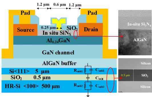
Figure 1: Cross-sectional structure of in-situ SiNx/AlGaN/GaN MISHEMT on SOI substrate.
This structure was grown both on 500μm SOI and 1000μm high-resistivity silicon substrates. The fabricated MISHEMTs (Figure 1) were mesa isolated with annealed titanium/aluminium/nickel/gold ohmic contacts and nickel/gold T-gates. The gate length was 0.25μm. The gate was centered in the 3μm source-drain gap. The devices were completed with plasma-enhanced chemical vapor deposition (PECVD) and etching of SiNx passivation.
Hall-effect measurements showed the material on SOI to have better performance than that on high-resistivity silicon (Table 1). The MISHEMT performances also suggested reduced numbers of interface traps: 1.13x10¹²/cm2-eV on SOI compared with 1.71x10¹²/cm2-eV on high-resistivity silicon. The researchers attribute the improvements to improved structural quality and reduced buffer trapping.
Table 1: Hall-effect measurements.
| Substrate | SOI | HR Si |
| Two-dimensional electron gas density | 1.02x10¹³/cm2 | 9.2x10¹²/cm2 |
| Mobility | 1605cm2/V-s | 1533cm2/V-s |
| Sheet resistance | 392Ω/square | 419Ω/square |
Raman spectroscopy suggested that the GaN on SOI was strain-relaxed compared with the GaN on HR silicon. X-ray analysis indicated smooth layer surfaces and abrupt interfaces between layers. Atomic force microscopy showed a smoother SiNx surface of 0.318nm root-mean-square roughness for the SOI sample, compared with 0.34nm for the HR Si structure.
Electrically, the use of SOI substrates improved the off-state leakage by more than one order of magnitude over the HR Si MISHEMTs. In both cases, the dominant leakage route was through the buffer. The subthreshold swing was 0.39V/decade (390mV/decade) for the MISHEMTs on SOI, compared with 0.44V/decade for HR Si. The maximum drain current and transconductance were found to be 15% and 13% higher, respectively, in the devices on SOI. The researchers attribute the improvements to the enhanced mobility on SOI. The devices were normally on at 0V gate potential with pinch-off voltages at -6.6V and -6V for the SOI and HR Si substrates, respectively.
At an increased temperature of 500K, the current flow in the MISHEMTs dropped due to scattering from lattice vibrations, according to the team.
Three-terminal breakdown measurements were made on devices with a 6μm source-drain gap. The gate potential was at -12V in the pinch-off region. The MISHEMTs on HR Si had an off-state leakage five times that of the device on SOI below 200V drain bias. With a 1mA/mm leakage criterion, the breakdown (VBR) was at 315V drain bias for the MISHEMT on SOI, compared with 270V for the HR Si structure.
The researchers comment: “The superior performance of the SOI can be attributed to the suppression of electrons being injected from the Si substrate into the III-nitride/Si interface. Furthermore, the leakage current of traditional HR-Si substrates was dominated by space-charge-limited current conduction through the buffer/transition layers.”
The VBR2/Ron figure of merit (Ron, on-resistance) was 11.84MW/mm for the SOI MISHEMT, while the SOI device registered 6.56MW/mm.
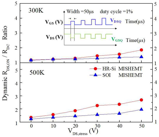
Figure 2: Dynamic switching performance determined with various stress voltages at 300K and 500K.
The SOI MISHEMT also demonstrated improved dynamic on-resistance performance under 50μs pulsed operation from the off-state (Figure 2). The increased dynamic on-resistance on HR Si was attributed to increased charge trapping in buffer states affecting performance.
Small-signal RF measurements gave cut-off/maximum oscillation (fT/fmax) frequencies of 32.1GHz/51.9GHz and 18.3GHz/25.4GHz for the SOI and HR Si MISHEMTs, respectively.
Large-signal 2.4GHz RF measurements in AB class amplifier operation gave maximum output powers of 660mW/mm and 550mW/mm for SOI and HR Si substrate MISHEMTs, respectively. The power-added efficiency reached around 30% for SOI and 20% for HR Si. “The increase of output power and the reduction of parasitic capacitances in MISHEMT on SOI provide a significant improvement in the device linearity,” the team adds.
AlGaN AlGaN MISHEMT SOI substrates MOCVD
https://doi.org/10.1109/TED.2017.2743229
The author Mike Cooke is a freelance technology journalist who has worked in the semiconductor and advanced technology sectors since 1997.


