


- News
27 September 2017
Deep-ultraviolet gallium nitride quantum dots in aluminium nitride
Cornell University and University of Notre Dame in the USA have achieved 40% internal quantum efficiency (IQE) for 219nm-wavelength deep-ultraviolet (UV) emissions from gallium nitride/aluminium nitride (GaN/AlN) heterostructures, according to temperature-dependent photoluminescence studies [S. M. Islam et al, Appl. Phys. Lett., vol111, p091104, 2017]. The researchers say that the 40% IQE is more than two times the highest reported value for AlGaN QW-based heterostructures at comparable short deep-UV wavelengths.
The researchers hope that their work will lead to rugged, portable, high-efficiency semiconductor light sources for deep-UV applications such as water/air purification, bio-photonic diagnostics, sterilization, food preservation, security and environment monitoring, and industrial curing.
Alloys of GaN and AlN cover the spectral range 365-205nm with energy bandgaps that support photon emissions between 3.4eV (GaN) and 6.02eV (AlN). The Cornell/Notre Dame team used GaN quantum dots (QDs) separated by AlN barriers to increase photon energies and shorten wavelength.
The molecular beam epitaxy (MBE) was carried out on 1μm AlN on sapphire templates (Figure 1). The templates were prepared in the MBE chamber by 7 hours outgassing at 200°C, and 2 hours at 450°C. The QDs were formed by depositing two monolayers of GaN separated by 4nm AlN barriers at 730°C. The barriers were grown using migration-enhanced epitaxy. Ten layers of QDs were grown on 30nm AlN buffer.
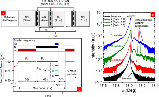
Figure 1: (a) Schematic of structure with 10 periods of ultra-thin GaN QDs in AlN barriers, (b) MBE growth diagram showing shutter sequence and relative III-V fluxes for 1 period of growth, and (c) high-resolution-x-ray diffraction (HR-XRD) ω-2θ scans showing signature of QD formation for sample A.
Stranski-Krastanov layer-plus-island growth was ensured by creating nitrogen-rich conditions through opening the Ga and N shutter simultaneously for 7 seconds. Dots were formed by interrupting the growth for 18 seconds after the GaN layer deposition, allowing the layer to decompose into islands.
The emission wavelength was dependent on the Ga/N ratio during MBE. X-ray analysis suggested sharp heterointerfaces between GaN and AlN material, with no intermixing to form AlGaN alloy.
At 5K temperature, the photoluminescence (PL) from the samples showed peaks at 234nm (A), 222nm (B), and 219nm (C) wavelengths. These short wavelengths constitute the highest reported photon energy emissions from GaN to date, 5.67eV for 219nm wavelength, according to the researchers. Raising the temperature to room conditions (300K) red-shifted the peaks by about 4nm.
Comparison with theoretical simulations suggested effective GaN thicknesses at 1.4 monolayer (A), 1ML (B), and 0.8ML (C). In line with these estimates, the PL intensity was lower for the shorter-wavelength and smaller GaN volumes of sample C. The simulations also suggested the confined structure was robust against the quantum-confined Stark effect (QCSE). In other words, the electric fields arising from spontaneous and strain-dependent charge polarization effects did not significantly reduce the overlap of the electron and hole wavefunctions. Large overlap is required for effective photon emission.
The simulations also resulted in estimates for linewidth broadening of 6nm (A), 30nm (B), and 36nm (C), which compared with actual measurements of 9 nm (A), 20 nm (B), and 19 nm (C).
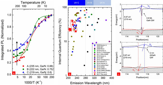
Figure 2: (a) Estimation of IQE from temperature-dependent integrated PL spectra (solid lines are shown as guide), (b) comparison of measured IQE with AlGaN based QWs, and (c) enhancement of IQE using GaN QWs due to reduced QCSE.
The IQE was estimated from the ratio of the 300K/5K PL, giving 20% for sample A and 40.2% for sample C (Figure 2). The researchers attribute the high IQE to the reduction of QCSEs. In contrast to AlGaN quantum well PL, the IQE trend increases for shorter wavelengths. The researchers add: “This is achieved because the reduction of the GaN QW/QD thickness enhances the overlap integral, reversing the trend of decreasing IQE at shorter wavelengths. Furthermore, the emission matrix element is converted to surface-emission, which is highly desirable for light extraction.”
http://dx.doi.org/10.1063/1.5000844
The author Mike Cooke is a freelance technology journalist who has worked in the semiconductor and advanced technology sectors since 1997.


