


- News
26 April 2018
Platform for fully vertical gallium nitride on silicon power devices
Massachusetts Institute of Technology (MIT) in the USA and Enkris Semiconductor Inc in China claim record performance for vertical gallium nitride (GaN) power diodes on foreign substrate [Yuhao Zhang et al, IEEE Electron Device Letters, published online 26 March 2018]. The researchers have developed a new platform for vertical GaN on silicon (Si) that creates a back-side trench, allowing a back contact to be made to the n-GaN layers.
The trench etching removes resistive buffer layers that have up to now mainly restricted GaN/Si power electronics to lateral or quasi-vertical structures with all contacts on the top side of epitaxial structures. The buffer layers are needed to bridge the lattice and thermal expansion mismatch between the foreign substrate and the GaN crystal structure. Fully vertical GaN power devices have generally been demonstrated on very expensive bulk or free-standing GaN substrates.
Vertical power devices are attractive because they push peak electric fields away from the surfaces and associated electron states that can cause premature breakdown. Vertical structures hence allow higher currents and voltages in more compact footprints. Also, lateral/quasi-vertical devices suffer from current crowding, which increases Joule heating.
The advantages of using silicon substrates are large diameter (8-inch) and low cost (less than $1/cm2). The researchers estimate the cost of 4-inch silicon carbide substrates at ~$5/cm2, while 2-inch GaN-on-GaN wafers cost ~$50/cm2.
The team believes that the trench process constitutes a potential platform for fully vertical power transistors and advanced diodes.
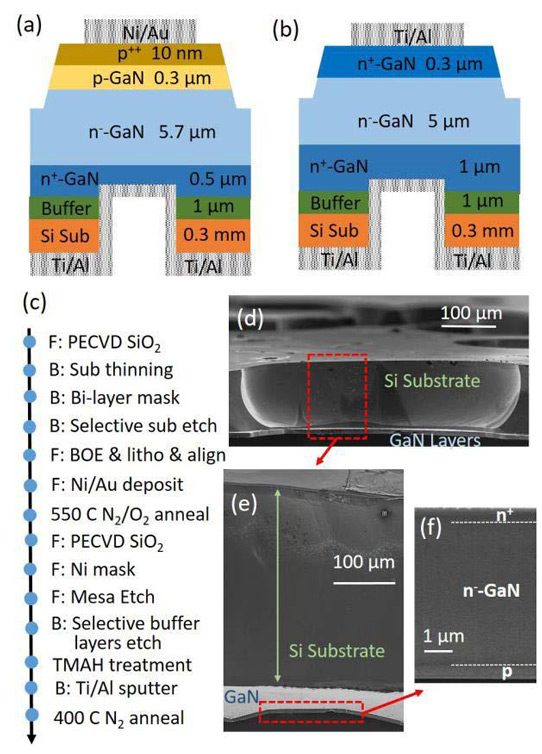
Figure 1: Schematic structure of (a) fully vertical GaN-on-Si pn diodes and (b) test device for backside trench etch and contact formation. (c) Main fabrication steps for fully vertical pn diodes. ‘F’ and ‘B’ represent front-side and back-side processes, respectively. Cross-sectional scanning electron microscopy (SEM) images of (d) circular back-side trenches, (e) silicon and GaN layers inside trenches and (f) GaN layers at trench bottom.
Enkris grew the epitaxial structure (Figure 1) on 6-inch-diameter (111) 1mm-thick silicon by metal-organic chemical vapor deposition (MOCVD). An optimized carbon doping was used in the n--GaN drift layer to compensate for background doping with a view to maintaining electron mobility and dynamic performance. The dislocation density was estimated through x-ray diffraction studies to be 2x10⁸/cm2 - “very low for GaN-on-Si wafers”, the researchers comment.
Device fabrication began with silicon dioxide deposition on the front side as protection. The silicon substrate was thinned to 300μm (0.3mm) with sulfur hexafluoride plasma etch. Further selective etching was used to remove all the silicon in the desired trench region.
The top-side silicon dioxide was removed before depositing an annealed nickel/gold (Ni/Au) ohmic contact. Selective etching of the top and bottom sides of the wafer created mesa isolation and removed the buffer layer so the back contact trench could be made, respectively.
Hot tetramethylammonium hydroxide (TMAH) treatment was used to remove surface damage and roughness from the plasma etch processing. After cleaning the etch mask materials, titanium/aluminium (Ti/Al) was sputtered and annealed to make the back ohmic contact.
The team fabricated pn diode devices with a 300μm-diameter circular backside trench and 350μm-diameter front-side anode. The larger anode was designed to compensate for the lower conductivity of p-GaN.
The on/off current ratio was 109 with a turn-on voltage (Von) of 3.1V for 10A/cm2 current density. The ideality factor was around 2 for low currents, indicating space-charge recombination. At higher current the ideality increased due to deep-level-assisted tunneling and p-GaN contact resistance (Ron), according to the researchers. At 3.7V, the specific differential on-resistance was less than 0.4mΩ-cm2.
The team comments: “These characteristics are significantly better than previous reports of GaN-on-Si vertical diodes, where the Von was around 3.5-4V and the Ron was extracted at a high bias of 5.5-9V.”
Increasing the temperature to 150°C increased the on-resistance to 0.85-0.95mΩ-cm2. The turn-on voltage was slightly reduced due to increased dopant activation in the p-GaN.
Room-temperature reverse breakdown (BV) occurred at 720V – at 500V the leakage was 10-2A/cm2 (10-1A/cm2 at 700V). The researchers claim these values are “at least 10-to-100-fold lower than the lowest leakage reported in quasi-vertical GaN-on-Si diodes so far”. They add: “The off-state leakage mechanism is dominated by the trap-assisted space-charge-limited current (SCLC), similar to previous reports of GaN-on-Si vertical diodes.” These previous vertical diodes managed reverse breakdown voltages of more than 350V.
The breakdown came a little earlier (680V) for 150°C conditions. The breakdown occurred at the mesa edges, so edge-termination field-plate/ring structures should be effective in increasing breakdown voltages.
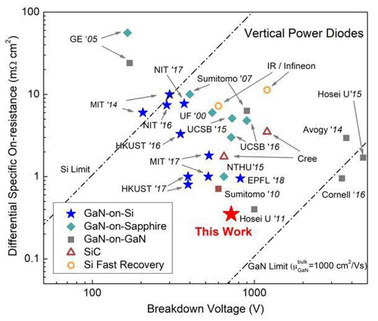
Figure 2: Specific on-resistance versus breakdown of vertical GaN power diodes on silicon, sapphire and GaN substrates and commercial 600V/1200V SiC power diodes (Cree CPW5-0650-Z050B/CPW5-1200-Z050B) and silicon fast recovery power diodes (IR IRD4CC17HB5/IRD3CH42DB6).
The researchers compared their devices with a wide range of alternative research and commercial devices (Figure 2). They write: “Our device shows a record performance for GaN-on-Si vertical power diodes with a power figure of merit (BV2/Ron) of 1.5 GW/cm2 . Our diodes also showed lower Ron than commercial SiC and Si power diodes at similar voltage classes.”
GaN GaN pn diodes Silicon power devices
https://doi.org/10.1109/LED.2018.2819642
The author Mike Cooke is a freelance technology journalist who has worked in the semiconductor and advanced technology sectors since 1997.


