


- News
9 April 2018
Silicon carbide superjunction Schottky junction diodes
China’s Zhejiang University claims the first functional silicon carbide (SiC) superjunction (SJ) device, in the form of a Schottky diode [Xueqian Zhong et al, IEEE Transactions On Electron Devices, vol65, p1458, 2018]. However, the device seems similar to a device presented by three members of the Zhejiang team at the 28th International Symposium on Power Semiconductor Devices and ICs (ISPSD) in 2016.
Superjunctions consist of vertical p- and n-type regions that, with perfect charge balancing, allows the drift regions of power devices to be depleted, increasing blocking voltages. In principle, this should allow SJ devices to beat the theoretical limits for unipolar power devices in terms of the trade-off between high breakdown voltage and low on-resistance.
The researchers comment: “It is expected that higher-voltage SJ devices based on SiC will offer more advantages over the conventional devices. Also, three-terminal devices are more favorable but their developments are even more challenging.”
The material used for the devices was an n-type 4°-offcut 4H-SiC substrate with a 12μm n-SiC epitaxial layer. Trenches 3μm wide (TW) and mesas 2μm wide (MW) were etched with inductively coupled plasma with a complex recipe to round corners and avoid subtrenches that can create the conditions for field crowding and premature breakdown (Figure 1).
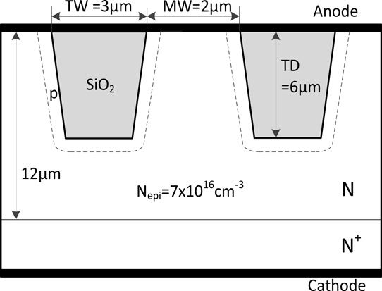
Figure 1: SiC-SJ Schottky diode cell structure with basic dimensions.
The trench wall angle was 86° to enable tilted implantation of aluminium p-type dopants and silicon dioxide refill. The implantation was carried out in a number of vertical and tilted steps to give a box profile. The depth of the doping was 0.5μm at the bottom of the trench and 0.3μm for the sidewalls. Nickel was used for a Schottky anode contact.
The optimum annealing temperature to activate the p-type doping was found to be 1350°C, which gave the highest breakdown voltage of 1350V. This breakdown figure was 95% of the simulated 1420V for a perfectly charge-balanced device.
The researchers suggest, based on simulations of the implant process, that lower-dose implants combined with higher annealing temperatures would be more effective in repairing implant damage to the crystal structure, giving better device performance in future work.
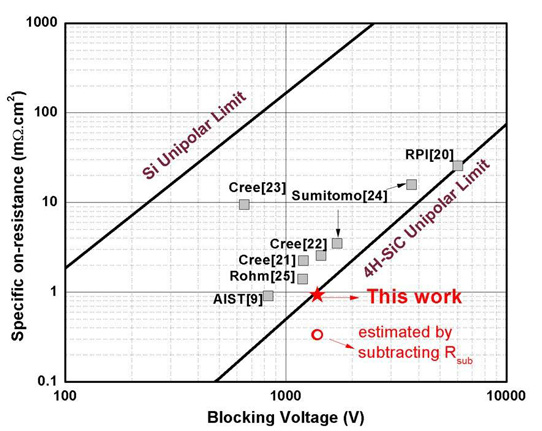
Figure 2: Trade-off between breakdown voltage and specific on-resistance in recent 4H-SiC-commercial products and research devices.
The devices underwent reversible avalanche breakdown. The forward current-voltage curve has a knee at about 1.3V, reflecting nickel’s work function. The specific on-resistance was 0.92mΩ-cm2 – about 0.6mΩ-cm2 of this is attributed to the substrate. By subtracting the substrate resistance, the researchers point out that the residue of 0.32mΩ-cm2 for the drift region breaks the theoretical limit for one-dimensional unipolar Schottky-junction SiC devices (Figure 2).
Silicon carbide Superjunction Schottky junction diodes
https://doi.org/10.1109/TED.2018.2809475
https://doi.org/10.1109/ISPSD.2016.7520820
The author Mike Cooke is a freelance technology journalist who has worked in the semiconductor and advanced technology sectors since 1997.


