


- News
23 August 2018
Photo-electro-chemical deep trench etching in gallium nitride
SCIOCS Co Ltd and Hosei University, both of Japan, have reported progress in using photo-electro-chemical (PEC) etching for deep high-aspect-ratio trenches in gallium nitride (GaN) [Fumimasa Horikiri et al, Appl. Phys. Express, vol11, p091001, 2018]. The team hopes that the technique will open up new device structures for power electronics, using GaN’s high breakdown field and high electron drift velocity in high fields.
Deep etching is needed to create ‘superjunction’ structures with columns of p- and n-type material that, when incorporated into lateral field-effect transistors, enable breakdown voltages of more than 10kV. Vertical devices can also benefit from superjunction drift regions and other deep-etched structures. High-quality fast etch-rate processes are also desired for ridge fabrication of laser diodes, wafer-dicing applications, and micro-electro-mechanical systems (MEMS). PEC has already been applied to mesa, gate-recess, and vertical-cavity surface-emitting laser (VCSEL) fabrication processes.
According to Horikiri, the work was supported by a big budget from Japan’s Ministry of the Environment. The team comments: “We commit to sharing this convenient PEC etching technology with the GaN community as part of our responsibility as a supplier of GaN substrates.”
Normally, deep etching is achieved with dry plasma etching such as inductively coupled plasma reactive-ion etch (ICP-RIE), which suffers from high surface damage. Further problems arise from low dry-etch selectivity between GaN and mask materials. High-quality etch techniques tend to be slow, reducing the scope for deep structures.
The researchers prepared 2-inch free-standing GaN substrates by void-assisted separation of n-type hydride vapor phase epitaxy (HVPE) material from sapphire [Mike Cooke, Semiconductor Today, p80, June/July 2018] - a technique developed by SCIOCS. The dislocation density in the wafer was in the range 2x10⁶/cm2 to 5x10⁶/cm2.
Further diode layers were grown by metal-organic vapor phase epitaxy – 5.8µm n-GaN for Schottky barrier diodes and 2µm n+-GaN, 10µm n--GaN, 500nm p-GaN and 20nm p+-GaN for pn diodes. The pn diode material was annealed at 850°C for 30 minutes in nitrogen to activate the magnesium acceptors of the p-type layers. The effect of annealing was to drive out the hydrogen atoms that passivate the acceptors.
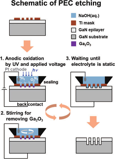
Figure 1: PEC etch scheme.
The mask material for the PEC etch (Figure 1) was titanium. PEC etching uses “photo-assisted anodic oxidation” to etch GaN. The process releases Ga3+ from GaN with the positive charge coming from holes generated by ultraviolet (UV) light at the GaN/electrolyte anodic interface. The electrons are removed by the electrical circuit of the PEC set up between an ohmic contact on the back-side of the GaN wafer and a platinum counter-electrode as cathode. The etch potential was 1V. The UV radiation was provided by a mercury-xenon lamp, giving 9.0mW/cm2 at vertical incidence. The radiation and etch potential were operated in pulse mode with 0.6 duty cycle on the potential.
The electrolyte contained OH- hydroxide ions that react with the Ga3+, forming Ga2O3. The electrolyte solution contained 0.01M sodium hydroxide and 1% Triton X-100 [C14H22O(C2H4O)n ; 4-(1,1,3,3-tetramethylbutyl)phenyl–polyethylene glycol] as wetting agent, reducing surface tension and assisting in bubble removal.
The PEC process achieved a smooth surface rate of 24.9nm/minute, comparable with damage-free dry etching. Increasing the PEC rate to 175.5nm/minute resulted in a rough surface. Higher-speed PEC could find uses in wafer dicing.
With a 50nm-thick titanium mask consisting of 90µm-diameter circular dots, PEC etching to a depth of 20µm gave a selectivity of greater than 400 (20µm/50nm). Side etching was less than 1µm.
In experiments on trench etching, the depth reached was controlled by current density rather than mask orientation along the m- or a-axes of the GaN lattice. The trench etch rate of short-width aperture masks slowed at about 30µm depth. The researchers suggest that this was due to the difficulty for the UV radiation to reach the etch front at the bottom of the trench. They add that a coherent UV source might help in deep trench etching.
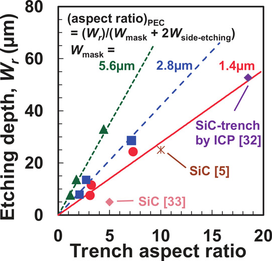
Figure 2: Relationship between PEC etching depth and trench aspect ratio. Solid, dashed and dotted lines correspond to estimates based on aspect ratio of PEC with trench width that includes side-etching of the order 0.7µm into both walls. Filled symbols show experimental results.
The maximum trench aspect ratio achieved was 7.3 with 3.3µm width and 24.3µm depth (Figure 2). The team comments: “This aspect ratio and the etching depth are comparable to the best results for SiC trenches fabricated by ICP-RIE, and they indicate the excellent potential of PEC etching not only in the fabrication of optical and electronic devices, but also in fabricating GaN-MEMS such as the through-via of wafers, diaphragms, microfluidic channels, and optical gratings.”
Photo-electro-chemical etching GaN Laser diodes MEMs VSCELs
https://doi.org/10.7567/APEX.11.091001
The author Mike Cooke is a freelance technology journalist who has worked in the semiconductor and advanced technology sectors since 1997.


