


- News
29 August 2018
Atomic-layer sidewall passivation of indium gallium nitride μLEDs
University of California Santa Barbara (UCSB) in the USA has improved the performance of indium gallium nitride (InGaN) micro-sized light-emitting diodes (μLEDs) through atomic layer deposition (ALD) of sidewall passivation [Matthew S. Wong et al, Optics Express, vol26, p21324, 2018].
Unpassivated sidewalls can be a source of LED inefficiencies through electron-hole recombination into photons being diverted into non-radiative surface recombination at dangling bonds and surface-roughness defects arising from dry plasma etching. Sidewall recombination becomes more influential as devices become smaller, impacting efficiency. Conventionally, plasma-enhanced chemical vapor deposition (PECVD) is used to apply passivation. The UCSB team has found that ALD-passivated μLEDs had better performance than PECVD-passivated devices.
μLEDs demonstrate long operating lifetime, high luminous efficiency, and chemical robustness. Applications include their use as pixels in displays – both in large-area and in near-eye head-mounted varieties. Monochrome μLED displays have demonstrated high resolution, efficiency and contrast ratio. The small size of μLEDs can also enable higher-speed operation for high-speed gigahertz-modulation-bandwidth visible-light communication.
Table 1. Structural details of μLED
| Layer | Thickness |
| Magnesium-doped p+-GaN | 17nm |
| Magnesium-doped p-GaN | 120nm |
| Magnesium-doped AlGaN EBL | 26nm |
| 6x InGaN/GaN MQW | 2.4nm/22nm |
| 30x silicon-doped InGaN/GaN | 3nm/3nm |
| Silicon-doped n-GaN | 4μm |
| Unintentionally-doped GaN | 1.4μm |
Epitaxial structures were grown on sapphire by metal-organic chemical vapor deposition (MOCVD) – see Table 1. Square μLEDs were fabricated (Figure 1), beginning with an electron-evaporated indium tin oxide (ITO) transparent conductor on the top p-GaN layer. The square mesas of the μLEDs were formed using reactive-ion etching down to the n-GaN layer.
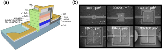
Figure 1: (a) Cross-sectional schematics of μLED design and (b) scanning electron microscope images of six μLEDs.
An omni-directional reflector (ODR) was created using ion-beam deposition of silicon dioxide and tantalum pentoxide, capped with aluminium oxide. The dielectric ODR both reflected light from the metal layers and electrically isolated the n- and p-contacts. The reflectance of the ODR was 95.5% in the blue wavelength range 430-450nm.
Passivation consisting of 50nm silicon dioxide was applied by using either PECVD or ALD processes. Windows for aluminium/nickel/gold contacts were cut into the passivation by hydrofluoric acid (HF) or inductively coupled plasma (ICP) etch.
The μLEDs were singulated into 750μmx750μm dies. The test devices were mounted on silver headers with wire bonding and resin encapsulation.
Four types of μLED were produced: 1) without sidewall passivation, 2) with ICP-etched ALD passivation, 3) HF-etched PECVD passivation, and 4) HF-etched ALD passivation. Missing from this list were ICP-etched PECVD passivation devices. Such devices were found to have extremely low light output and poor electrical performance.
For the unpassivated μLED-1, the larger area device (>60μmx60μm) light output crowded towards the edges. The light output became more uniform in the smaller devices due to better current spreading in the ITO transparent oxide. However, the light output density was lower in the sub-60μmx60μm LEDs due to the increased influence of non-radiative surface recombination from etch damage and non-passivation.
μLED-2 and μLED-4 demonstrated uniform light emission for all sizes between 10μmx10μm and 100μmx100μm. Also, the density of light emission remained high for all sizes. This was in contrast to μLED-3 (PECVD passivation), whose light emission became very dim for the smaller devices. The emission was also non-uniform for the brighter, larger devices.
The passivation also increased light extraction – the higher index of refraction of the dielectric compared with air increases the critical angle for total internal reflection in the III-nitride material, allowing more photons to escape. The light output was increased in 20μmx20μm μLEDs-2 and -4 by about 40% over the unpassivated μLED-1 at 20A/cm2 current density injection. At 95A/cm2 the improvement was 20%.
The PECVD passivation of μLED-3 suffered from reduced transparency of the ITO layer, according to the researchers. The PECVD process releases hydrogen radicals that attack the ITO material, leaving metallic indium and tin oxide. The use of metal-organic precursors in the ALD process avoids the generation of hydrogen radicals.
Current leakage under -4V reverse bias was least for μLED-4 at all device sizes. The density of current leakage increased for smaller devices due to the device sidewall area/volume ratio being greater.
Scanning electron microscope (SEM) inspection suggested that the ICP etching damaged the ITO layer more than the HF process. The HF etch is more selective to silicon dioxide over ITO than ICP. The ITO damage introduced extra current leakage over that of the HF process.
The peak external quantum efficiency (EQE) of 100μmx100μm devices ranged from 36% to 41% (Figure 2). The peak came around the same injection current density of~5A/cm2. The EQE drooped to around 25% at 100A/cm2. There was a wider spread of EQEs in the mid-range and the μLED-4 process initially drooped more quickly.
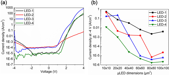
Figure 2: (a) Current density-voltage characteristics from −4V to + 4V of 20μmx20μm μLEDs with different sidewall passivation techniques and (b) dependence of leakage current at −4V on dimensions of μLEDs with different sidewall passivation methods.
For 20μmx20μm μLEDs, the EQE was lower (33% for μLED-4) but the droop effect was also much reduced - in μLEDs-4 and -2 almost absent, and for μLED-3 the EQE increased up to 100A/cm2. The unpassivated μLED-1 showed a more conventional 40% droop and the peak efficiency was only 24%. The researchers attribute the improvement in the passivated μLEDs-2/-4 to increased light extraction and reduced leakage current.
https://doi.org/10.1364/OE.26.021324
The author Mike Cooke is a freelance technology journalist who has worked in the semiconductor and advanced technology sectors since 1997.


