


- News
5 December 2018
Gallium oxide trench Schottky barrier diodes with ultra-low leakage
Cornell University in the USA and Japan’s Novel Crystal Technology Inc claim the lowest leakage current yet reported for monoclinic beta-polymorph gallium oxide (β-Ga2O3) Schottky barrier diodes (SBDs) [Wenshen Li et al, Appl. Phys. Lett., vol113, p202101, 2018]. The low leakage current density of less than 1μA/cm2 was combined with a relatively high breakdown voltage of 1232V. The devices used a trench structure to create fins with a metal-insulator-semiconductor (MIS) stack on the sidewalls to reduce surface field effects, suppressing leakage under reverse bias.
Gallium oxide has many properties useful for high-power electronic and radio-frequency amplifier applications: a wide bandgap of 4.5eV implying a high critical electric field of up to 8MV/cm, and a reasonable electron mobility of the order 200cm2/V-s. Such devices could also be designed to operate under harsh and high-temperature conditions. Melt-growth methods enable the commercial production of single-crystal bulk Ga2O3 substrates.
The researchers used halide vapor phase epitaxy (HVPE) to create the device layers of the SBD (Figure 1). The fin area ratio was ~60% of the total fin+trench pitch. In simulations, a narrower fin was expected to result in lower electric fields near the top surface. The 10μm drift layer had a uniform net doping of 2x10¹⁶/cm3 that made a significant contribution to the improved performance.
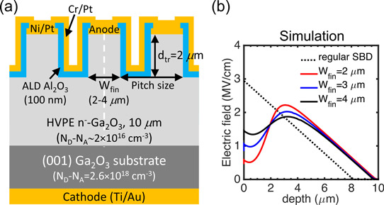
Figure 1: (a) Schematic cross section of β-Ga2O3 trench Schottky barrier diodes. (b) Simulated electric field profile at reverse bias of 1200V along dashed vertical cut line at center of fin in (a).
Fabrication began with formation of the back cathode: first reactive ion etch (RIE) was performed to improve the ohmic nature of the contact, followed by evaporation and annealing of the titanium/gold (Ti/Au) contact metal.
The front-side of the epitaxial wafer was patterned, using nickel/platinum (Ni/Pt) as both the hard mask for trench RIE etching and the Schottky contact of the final device. The trenches were etched to a depth of 2μm with the fin channels oriented along the [010] direction. The fin sidewalls are described as being ‘near vertical’.
The trenches were lined with aluminium oxide (Al2O3) applied using atomic layer deposition (ALD). Dry etch through the aluminium oxide at the tops of the fins exposed the nickel/platinum Schottky contacts. The device was completed by sputtering chromium/platinum (Cr/Pt) on the trench sidewalls.
The researchers also produced Ni/Pt Schottky diodes without the fin structuring, for comparison. The current densities were calculated based on device, not fin, area. The ideality factor of both devices was 1.08. The trench SBDs had a Schottky barrier height of 1.40eV, compared with 1.35eV for the regular device. The increased effective barrier height was attributed to the adjacent metal-oxide-semiconductor junction on the sidewalls of the trenches.
Pulsed measurements were used to avoid self-heating effects. The restricted area of the current flow through the fins resulted in reduced current density compared with the regular device. The specific differential on-resistance of the trench SBD was 15mΩ-cm2, compared with 6.6mΩ-cm2 for the regular device.
The trench SBD also suffered from trapping effects in voltage scans not seen in the regular device. The research infer that “the trapping must be located at the trench MIS structure”. The trapped charge increases the depletion in the fin, constricting current flow. The researchers estimate the extra depletion thickness to be of the order 170nm at zero bias, assuming a trapped electron sheet density of ~8x10¹¹/cm2.
The researchers suggest that the trapping could be reduced with a post-deposition anneal (PDA) of the Al2O3 dielectric and with improved surface treatment on the Ga2O3 surface after the dry etch.
The place where the trench SBD performed better was under reverse bias with breakdown at 1232V, compared with 734V for the regular device. The fins of the best trench SBD were 2μm wide. The leakage current before breakdown was less than 1μA/cm2, and when the reverse bias was below 1000V the leakage was less than 0.1μA/cm2, corresponding to power dissipation less than 0.1mW/cm2. Wider-finned devices had higher leakage and lower breakdown voltages.
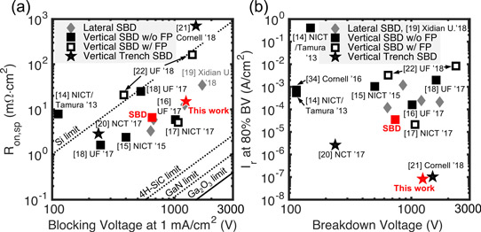
Figure 2: Benchmark plots of state-of-the-art β-Ga2O3 SBDs. (a) Differential specific on-resistance (Ron,sp, excluding turn-on voltage) versus blocking voltage specified at reverse leakage current density of 1mA/cm2. (b) Leakage current density at 80% of reported breakdown versus reported hard-breakdown voltage.
The team compared the performance of its devices with other reports (Figure 2). The specific differential on-resistance compared with the blocking voltage at 1mA/cm2 current density showed ‘notable’ improvement over previously reported trench devices, while also giving comparable performance to the best reported β-Ga2O3 SBDs. The team comments: “In comparison with our previous results, the on-resistance is much reduced due to a more uniform doping profile with a moderate level (~2x10¹⁶/cm3) and less carrier compensation.”
Comparison was also made between the reverse leakage at 80% of breakdown and the breakdown voltage itself, showing lower leakage in the trench SBDs, compared with regular devices. The researchers claim the lowest leakage reported for the SBDs with 2μm-wide fins. The team’s regular SBD showed similar performance to other reports. The lower leakage is therefore likely attributable to the trench structure itself.
The team expects progress toward the theoretical material limit for Ga2O3 through reduced trapping in the MIS structure and better field management.
Monoclinic beta-polymorph gallium oxide Schottky barrier diodes HVPE
https://doi.org/10.1063/1.5052368
The author Mike Cooke is a freelance technology journalist who has worked in the semiconductor and advanced technology sectors since 1997.


