


- News
31 December 2018
Increasing current performance in III-nitride p-channel transistors
Cornell University and Intel Corp in the USA claim simultaneous records for on-current and on/off current ratio for enhancement-mode p-channel field-effect transistors (pFETs) based on a two-dimensional hole gas at a gallium nitride/aluminium nitride (GaN/AlN) interface [Samuel James Bader et al, IEEE Electron Device Letters, published online 5 October 2018].
Producing effective p-channel transistors in GaN-based devices would open up the potential of energy-efficient complementary p-/n-channel circuits. Unfortunately, such a development is hampered by the poor characteristics of hole transport in III-nitride materials relative to much higher-mobility electrons.
While the wide bandgaps of GaN and AlN are attractive from the perspective of power and radio-frequency electronics, this same property is at the root of the sluggish nature of hole transport. Wide gaps are associated with a large effective hole mass and low mobility. The wide gap also implies a deep valence band and generating holes is difficult since the best acceptor doping is provided by magnesium, which has an activation energy of the order 200meV, an order of magnitude higher than the typical thermal excitation energy at room temperature (~26meV). This makes the hole density exponentially smaller than the doping concentration.
A further challenge is providing enhancement-mode ‘normally-off’ operation in transistors, which is beneficial both in terms of power consumption and for fail-safety in high-power applications.
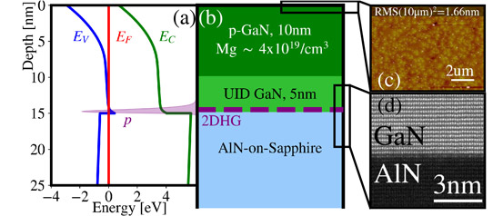
Figure 1: (a) Energy-band diagram and (b) layer structure of grown heterostructure. Holes (purple shade) are tightly confined to GaN/AlN interface, forming 2D carrier gas. (c) Atomic force microscope (AFM) scan, showing relatively rough (1.66nm root mean square) epi-surface due to high (for molecular beam epitaxy) doping levels, (d) cross-sectional transmission electron micrograph showing atomically abrupt GaN/AlN interface.
The structure (Figure 1) was grown on AlN-on-sapphire templates. Van der Pauw/Hall measurements gave 5.8x10¹³/cm2 hole density, 7.1cm2V-s mobility, and 15kΩ/square sheet resistance. The relatively low sheet resistance promises to reduce access and contact parasitics. The mobility of electrons in two-dimensional electron gas AlGaN/GaN structures is typically more than 1000cm2/V-s.
Simulations of the GaN/AlN structure gave an expected 5.3x10¹³/cm2 hole density. The simulations also predicted a low hole density in the overlying p-GaN of ~1011/cm2 due to the deep nature of the magnesium (Mg) acceptors with activation energy ~200meV. The bulk of the holes occur in the first couple of nanometers of the channel at the GaN/AlN interface, according to the model. This allows treatment of the charge carriers as belonging to a two-dimensional hole gas (2DHG). The high hole density is enabled by the large charge polarization difference between GaN and AlN.
The transistor structure was fabricated with mesa etching, source/drain ohmic contact deposition, and gate stack formation. The ohmic contacts consisted of 450°C annealed nickel/gold. The gate was recessed 10nm through the p-GaN layer. Recessing enables the gate region to be depleted, shutting off current flow at 0V gate potential, but not the access areas of the device.
The gate was insulated with 7nm silicon dioxide from atomic layer deposition (ALD) processing. The gate electrode was titanium/gold. Capacitance-voltage structures based on the gate stack revealed a negative threshold, suggesting a 2DHG with 4.5fF/µm2 on-state capacitance.
The pFETs achieved current saturation and reasonable gate control. With 7µm gate length, a drain current of 10mA/mm was achieved with -10V drain bias. This compares with the previous best report for enhancement-mode GaN/AlN pFETs of 4mA/mm with -40V drain bias in a 2µm gate device. At -10V bias, the previous pFET only managed 0.04mA/mm. The on/off current ratio of 104 for the new pFET is also an order of magnitude better than previously.
Enhancement-mode GaN/AlInGaN pFETs with short 1µm gates have achieved 10mA/mm, but the researchers hope that scaling down the gate from 7µm could provide even higher drive currents.
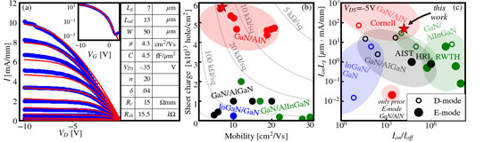
Figure 2: (a) Compact model (thin red) fitted to measured data (blue circles). (b) Sheet charge versus mobility for various reported III-nitride 2DHGs. (c) Benchmark of III-nitride pFET performance in terms of on-current and on/off current ratio.
The team attributes the high current-gate-length product (IonLg) to the low access and contact parasitics enabled by the low sheet resistance of the GaN/AlN structure (Figure 2). The researchers add: “The large bandgaps and band offset enable a thorough pinch-off, with the insulating AlN buffer preventing parasitic n- or p- leakage.”
Benchmarking against other reports shows the GaN/AlN approach to have significantly higher sheet charge, due to the charge polarization discontinuity. At the same time, hole mobility is comparable with most other approaches.
https://doi.org/10.1109/LED.2018.2874190
The author Mike Cooke is a freelance technology journalist who has worked in the semiconductor and advanced technology sectors since 1997.


