


- News
27 December 2018
Quantum dot laser diodes on CMOS-compatible on-axis silicon substrates
Hong Kong University of Science and Technology (HKUST) has developed its on-axis indium phosphide (InP) on silicon (Si) as a template for indium arsenide (InAs) quantum dot (QD) laser diodes emitting at ~1.5μm [Si Zhu et al, Appl. Phys. Lett., vol113, p221103, 2018].
The researchers hope that such C-band (1530–1565nm) lasers could become part of the growing opportunities for low-cost silicon photonic (SiPh) optoelectronic circuitry. The team used on-axis (001)-oriented Si, which is the preferred substrate material for mainstream complementary metal-oxide-semiconductor (CMOS) electronics. Often off-cut Si substrates are used to avoid anti-phase boundaries and other defects in InP buffer growth.
The C-band emissions cover the low-loss range of mid-/long-haul optical fibers and commercial erbium-dope fiber amplifiers (EDFAs) for dense-wavelength division multiplexing (DWDM) data transmission. QD structures have advantages over quantum wells in terms of optical performance and defect tolerance. The latter property is important in heterostructure growth where different lattice structure constants and thermal behaviors create strains that more easily generate dislocations.
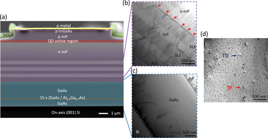
Figure 1: (a) Color-enhanced cross-sectional scanning electron microscope (SEM) image of whole epitaxial structure. Cross-sectional transmission electron microscope (TEM) images of (b) three stacks of 10-period InGaAs/InP strain layer superlattices (SLSs) with dislocation filtering effects identified by red arrows, (c) 2.2μm-thick GaAs intermediate buffer on nano-patterned V-grooved on-axis (001) Si substrate, and (d) plan-view TEM characterization of defect density of InP buffer on Si.
The substrates were prepared with V-grooves that relax misfit strain in the initial gallium arsenide (GaAs) buffer by creating twinned stacking faults (SFs) aligned to the {111} nucleation planes (Figure 1). The faults are then mostly trapped by silicon ridges at the head of the V-grooves.
When the GaAs growth from the grooves had coalesced, a 15-period superlattice of 5nm/5nm aluminium gallium arsenide (Al0.3Ga0.7As)/GaAs pairs gave a smooth growth front without pinholes or anti-phase boundaries.
After some more GaAs growth, an InP buffer was added, including three 10-period strained superlattices of 10nm/30nm In0.6Ga0.4As/InP as further dislocation filters. The superlattices were separated by 250nm InP spacers, grown at high temperature.
Plan-view transmission electron microscope (TEM) inspection gave a low defect density of 1.5x10⁸/cm2, compared with typical threading dislocation levels of 109-1010/cm2 for InP/GaAs without filtering. The team comments that the defect density is among the lowest reported defect density values for InP films grown on silicon substrates by metal-organic chemical vapor deposition (MOCVD).
The researchers optimized the five stacks of InAs quantum dot layers to reduce the inhomogeneous broadening of the photoluminescence by using a two-stage cap layer process. The first layer was 1.7nm In0.52Al0.29Ga0.19As grown at 510°C, the same temperature as the QDs. The second layer was 30nm 630°C In0.52Al0.29Ga0.19As.
The strongest peak was at 1512nm wavelength with 61.6eV linewidth. Although this was slightly wider than for QDs grown on InP substrate, the researchers say that their new material had over 4 times stronger peak intensity and 1.6 times narrower full-width at half maximum (FWHM) linewidth than previous batches of QDs on silicon.
There was also a number of other peaks that the team attributes to non-uniformity of QD sizes, as opposed to the effects of the stacking process. The areal density of QDs was ~4.5x10¹⁰/cm2.
The material was fabricated into standard ridge-waveguide edge-emitting lasers. The light-emitting/reflecting facets were cleaved and uncoated. The metal contacts were made on the epi-side since the III-V/Si interface had many defects, making it highly resistive to current flow.
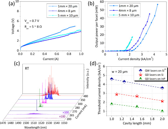
Figure 2: (a) and (b) Light output power-current-voltage (LIV) characteristics for three InAs/InAlGaAs/InP QD lasers grown on (001) Si substrate under pulsed operation at room temperature. (c) Emission spectra for 10μmx1000μm device at various injection currents. (d) Threshold current density distribution of optimized QD lasers on InP and Si, compared with QW lasers directly grown on (001) Si at varied cavity lengths (width 20μm).
The turn-on voltage of the device was 0.7V, while the laser threshold current density was 1.6kA/cm2 from a 5mmx10μm cavity (Figure 2). The light output power reached 57mW/facet without saturation.
The devices were characterized using pulsed injection – devices grown on InP substrates have been reported that can operate in continuous-wave mode. Also, the Si-based threshold currents are about twice that of QD laser diodes grown on InP substrates.
The team hopes that further improvement of InP-on-Si templates will close this performance gap. On the other hand, the QD devices show a factor of 1.6 reduction of threshold compared with the group’s previous quantum-well diodes on silicon. The team also reports that it has demonstrated wavelength tuning between 1478nm and 1523nm.
Varying the temperature of the devices between 20°C and 85°C, the researchers found the diode performance saturated around 10mW/facet at 80°C. The T0 characteristic temperature for the threshold current was extracted as 58.7K. This is described as “a reasonable value for InAs/InAlGaAs/InP QD lasers”. The researchers believe the T0 performance could be enhanced with p-type modulation doping. The wavelength stability of 0.3nm/K was found to be better than for QD lasers on InP.
The team comments on future prospects: “On-going work will be first focused towards continuous-wave (CW) operation by adopting the tunnel injection structures, in which QDs are separated from an InGaAs QW by an ultra-thin InAlGaAs barrier for more efficient carrier injection. Also, increasing the indium composition in the InGaAs interlayers to introduce a larger strain field would be beneficial for enhanced dislocation filtering. Additional structures like slotted grating couplers can be adopted forcing the light down from the epitaxial laser to the silicon waveguide to integrate with the existing SiPh circuits.”
InP InP on silicon InAs InAs quantum dot laser diodes MOCVD CMOS
https://doi.org/10.1063/1.5055803
The author Mike Cooke is a freelance technology journalist who has worked in the semiconductor and advanced technology sectors since 1997.


