


- News
28 December 2018
Improving ohmic contacts in III-nitride high-electron-mobility transistors
The Indian Institute of Technology Bombay reports improved performance of III-nitride high-electron-mobility transistors (HEMTs) by a change in the composition of the source and drain ohmic metal contacts [Yogendra K. Yadav et al, IEEE Electron Device Letters, published online 29 November 2018]. The researchers compared a standard metal contact structure of titanium/aluminium/nickel/gold (‘Ti/Al’) with their new recipe of titanium/gold/aluminium/nickel/gold (‘Ti/Au’).
The Ti/Au contacts demonstrated low contact resistance and sharper edges that allowed the source–drain separation to be significantly reduced. The researchers explain: “Low contact resistance, sharp edge acuity and small source–drain separation is key for high-power and high-frequency applications.”
The researchers worked on III-nitride material grown by metal-organic chemical vapor deposition (MOCVD) on silicon carbide (Figure 1). The barrier layer was aluminium gallium nitride (AlGaN). Transmission-line method (TLM) and HEMT metal contact structures were fabricated on the material. Mesa isolation was achieved by inductively couple plasma etch.
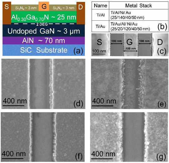
Figure 1: (a) Device schematic, (b) metal stacks, (c) SEM image of low source–drain separation HEMT; (d) & (e) SEM image of Ti/Al before and after annealing; (f) & (g) SEM image of Ti/Au before and after annealing.
The ohmic source–drain metal contacts were subject to annealing at 830°C-for 30 seconds in nitrogen. The HEMT structures included a nickel/gold Schottky gate: 100nm long with two 50μm wings, giving a total width of 100μm.
Scanning electron microscope (SEM) inspection showed that the Ti/Al structure suffered from significant lateral diffusion during annealing. The Ti/Au, by contrast, showed much sharper edge acuity.
Using the TLM structures, the researchers determined contact and sheet resistances: for Ti/Al, 0.67Ω-mm and 417Ω/square, respectively; for Ti/Au, 0.50Ω-mm and 420Ω/square.
On the basis of x-ray photoelectron spectroscopy (XPS), the researchers believe that the gold in the Ti/Au extracts gallium from the underlying III–nitride material, enabling the formation of more uniform TiN in the interface region during annealing.
As was to be expected, reducing the source–drain distance in the HEMT devices decreased the on-resistance (RON). At the same time, the breakdown voltage was also reduced due to the increased electric field. Knock-on effects of reduced on-resistance were increased saturation drain current at 0V gate potential (IDS,sat) and peak transconductance (gm). In frequency-dependent measurements, the lower resistance also enabled a higher unity current gain frequency (fT).
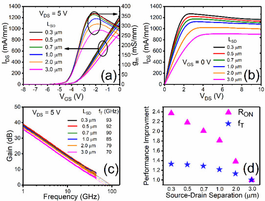
Figure 2: (a) Transfer characteristics of 0.100μmx100μm AlGaN/GaN HEMT at 5V drain bias. (b) Drain current–voltage (IDS–VDS) characteristics at 0V gate potential (VGS). (c) Current gain (|h21|) (d) Performance improvement with source–drain separation scaling.
The sharper edge acuity of the Ti/Au contacts enabled source–drain distances to be reduced to 300nm (Figure 2). This resulted in a number of performance improvements compared with 3μm separation (Table 1).
Table 1. Comparison of HEMTs with 3μm and 300nm source–drain separation.
| Source–drain separation | 3μm | 0.3μm |
| RON | 3Ω-mm | 1.;25Ω-mm |
| gm at 5V VGS | 276mS/mm | 365mS/mm |
| IDS,sat | 906mA/mm | 1230mA/mm |
| fT | 70GHz | 93GHz |
http://dx.doi.org/10.1109/LED.2018.2884155
The author Mike Cooke is a freelance technology journalist who has worked in the semiconductor and advanced technology sectors since 1997.


