


- News
12 December 2018
Lateral graphene/hexagonal boron nitride heterostructures
Xiamen University in China and University of Texas at Austin in the USA have developed a chemical vapor deposition (CVD) technique to grow two-dimensional heterostructures of hexagonal boron nitride (h-BN) and graphene (Gr) [Pingping Zhuang et al, Nanotechnology vol30, p03LT01, 2019]. Both h-BN and Gr adopt the hexagonal planar arrangement in monolayer two-dimensional sheets of atoms.
The researchers hope that the material could illuminate potential properties and effects such as electronic phase reconstruction across the one-dimensional h-BN/Gr interface, spin asymmetry induced magnetism, and topological ballistic transport.
Although the graphene domains were randomly distributed in terms of size, shape, and density, the potential for heterostructure-embedded electronic devices is enabled by the large-area uniform continuous films of CVD, compared with the laboratory-scale manipulation of micron-scale flakes seen in most device research reported so far. The researchers comment: “Further studies focusing on controllable growth based on this method are required to meet the device fabrication requirement.”
The team used electro-polished carbon-containing copper (C-copper) foil as a substrate for the CVD of h-BN from aminoborane (NH2BH2) and borazine (B3H6N3 in a benzine-like ring, hence the common designation as ‘inorganic benzene’) precursors in hydrogen carrier gas (Figure 1).
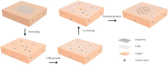
Figure 1: Schematic flow of lateral Gr/h-BN heterostructure growth on C-copper foils assisted by hydrogen etching.
The precursors were supplied by the decomposition of heated ammonia-borane (BH3NH3, AB) powders in a water bath. The C-copper foil was annealed before CVD at 1035°C to remove residual chemicals from the electro-polishing process (the reverse of electro-chemical deposition).
The hydrogen flow was maintained after the h-BN CVD, allowing partial etch of the film. Then, as the system was cooled, carbon atoms in the foil migrated to the edges of the h-BN structure, forming graphene domains in the gaps caused by hydrogen etching.
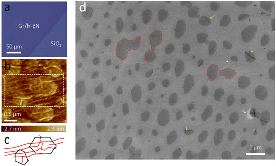
Figure 2: (a) Optical image of sample transferred to (PMMA). (b) AFM image of Gr/h-BN heterostructure. (c) Schematic outline of 1D interfaces (black) and wrinkles (red), which correspond to white-dashed rectangle marked area in (b). (d) SEM image of heterostructure transferred to silicon dioxide/silicon substrate. Aggregated graphene regions (red polygon), wrinkles (yellow arrow), and fracture (white arrow) are marked.
Under ultraviolet and visible radiation, the h-BN/Gr material transferred to quartz (SiO2) showed absorption peaks at 6.1eV and 4.2eV. The higher-energy photons were associated with the h-BN material, while the 4.2eV signal was attributed to the π plasmon peak in graphene. The researchers estimated a ‘Tauc’ optical bandgap for the h-BN/Gr combination of ~5.8eV.
Other analyses were carried out on the material: Raman spectroscopy, atomic force microscopy (AFM), scanning electron microscopy (SEM), and x-ray photoelectron spectroscopy.
Graphene Boron nitride heterostructures CVD
https://doi.org/10.1088/1361-6528/aaeb75
The author Mike Cooke is a freelance technology journalist who has worked in the semiconductor and advanced technology sectors since 1997.


