


- News
7 February 2018
Microwave deposition of gallium oxide on III-nitride on silicon substrate
The Indian Institute of Science has been developing microwave polycrystal deposition of β-phase gallium oxide (Ga2O3) on gallium nitride (GaN) on silicon with a view to application in deep ultraviolet (UV) optoelectronics [Piyush Jaiswal et al, Appl. Phys. Lett., vol112, p021105, 2018]. The team also demonstrated a visible-blind 230nm deep UV photodetector based on the β-Ga2O3 material.
The wide bandgap (4.9-5.3eV) of β-Ga2O3 could be useful for both deep UV and high-voltage applications. The absorption edge for β-Ga2O3 is in the wavelength range 240-250nm. Meanwhile, GaN has been developed for visible and near-UV light emission, along with, more recently, high-voltage and high-current-density electronics and for operation at high switching speeds. Bringing these technologies together, the researchers target heterostructures and devices that would exploit bandgap engineering opportunities.
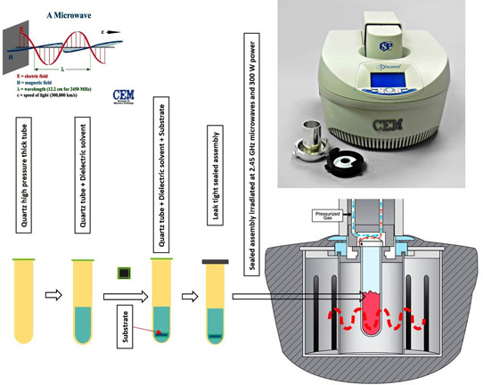
Figure 1: Schematic representation of microwave-irradiation-assisted film deposition process.
The Ga2O3 was deposited on III-nitrides by microwave irradiation of a reactant solution containing Ga(III)acetylacetonate, a β-ketonate complex (Figure 1). The solvent was a mix of ethanol and 1-decanol. The substrate was a GaN stack with aluminium gallium nitride (AlGaN) layers typically designed for high-electron-mobility transistors (HEMTs).
“Epitaxially grown GaN layers were used as substrates, because of the close lattice match between h-GaN and β-Ga2O3 along the (100) direction,” the team comments. Temperatures during the deposition did not exceed 200°C. The duration was less than an hour, including ramp up and ramp down.
X-ray photoelectron spectroscopy (XPS) of the β-Ga2O3 did not find any nitrogen, suggesting uniform coverage of the III-nitride layers. Further findings were some carbon from the organic solvents and an oxygen deficiency leading to vacancies and an expectation of n-type conductivity.
X-ray diffraction studies suggested a nano-crystalline Ga2O3 structure with an estimated thickness of 70-80nm. The average crystallite size was 3.3nm and the material was in the γ-phase. Rapid thermal annealing at 950°C for 10 minutes converted the phase to β with 22.4nm crystallites.
The researchers comment: “The counter-intuitive formation of γ-Ga2O3 at sub-200°C is attributable to locally elevated temperatures in the irradiated solution and to the nucleation kinetics of γ-Ga2O3 formation because γ-Ga2O3 has a spinel structure associated with many vacancies, and crystals containing vacant sites are stabilized at low crystallization temperatures.”
The x-ray results were backed up by scanning electron microscopy (SEM) and atomic force microscopy (AFM).
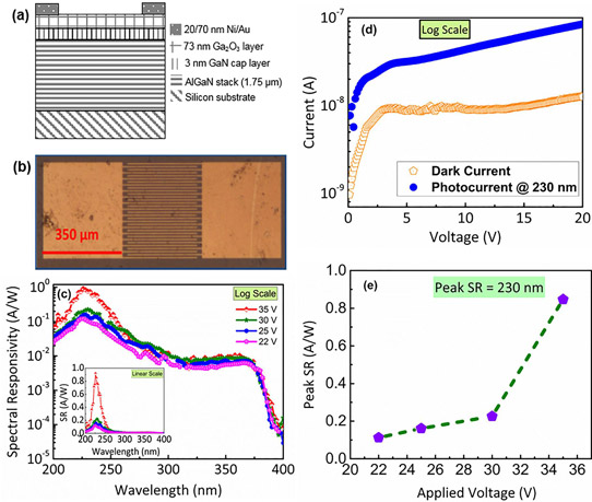
Figure 2: (a) Schematic of AlGaN/GaN HEMT stack (side-view). (b) Optical micrograph of fabricated MSM device (top-view). (c) Variation of spectral response (SR) with wavelength on log scale as function of bias. Inset: variation of SR with wavelength as a function of bias on a linear scale. (d) Variation of dark current and photocurrent with applied bias. Photocurrent was measured under 230nm illumination. (e) Variation of peak responsivity (SR at 230nm) with applied bias (measured at an optical chopping frequency of 30Hz).
Nickel/gold Schottky contacts were deposited on the β-Ga2O3 layer to create a metal-semiconductor-metal photodetector (Figure 2). The electrodes consisted of 16 interdigitated fingers. The width of the fingers was 5μm and the spacing was 6μm. The active area is given as 250μmx300μm.
Peak spectral responsivity occurred at 236nm deep UV – 0.1A/W at 22V bias and 0.8A/W at 35V. Compared with the response at 400nm visible wavelengths, the rejection ratio was more than 103 at 22V bias. The kink downward in the response at 365nm near-UV is attributed to absorption and conduction in the narrower ~3.4eV bandgap GaN layer beneath the β-Ga2O3. The dark current at 20V was ~12nA, compared with ~82nA under 230nm illumination.
The researchers suggest that the increase in peak response at 35V was due to internal gain. The team explains: “This gain comes from either an oxygen-deficient film, leading to trapping of holes in bulk, or interface states at the metal-semiconductor (M-S) Schottky junction enabling hole trapping at the M-S junction itself. As the M-S junction has to maintain charge neutrality, more electrons have to flow from the metal side, subsequently lowering the Schottky barrier, thereby leading to gain in the photodetector.”
Microwave polycrystal deposition β-phase gallium oxide GaN Deep ultraviolet
https://doi.org/10.1063/1.5010683
The author Mike Cooke is a freelance technology journalist who has worked in the semiconductor and advanced technology sectors since 1997.


