


- News
23 February 2018
Panasonic develops insulated-gate MIS GaN power transistor capable of continuous stable operation
© Semiconductor Today Magazine / Juno PublishiPicture: Disco’s DAL7440 KABRA laser saw.
Panasonic Corp of Osaka, Japan has developed an insulated-gate metal-insulator-semiconductor (MIS) gallium nitride (GaN) power transistor capable of continuous stable operation with no variation in its threshold gate voltage. This makes it possible to further increase GaN power transistor speed, enabling the miniaturization of electronic equipment, says the firm.
MIS-type GaN power transistors are expected to be practical for use as next-generation ultrafast power devices. Meanwhile, Panasonic has been researching MIS gate structures as a future technology for further increasing operation speed. However, conventional MIS-type GaN power transistors suffer from hysteresis, and high-speed switching operation with high current and high voltage has not previously been achieved.
Panasonic has now confirmed the first continuous, stable operation of MIS-type GaN power transistors, at a drain current of 20A and with a breakdown voltage of 730V. With a significant increase in switching frequency (an OFF operation time of 1.9ns and ON operation time of 4.1ns), the miniaturization of peripheral passive components becomes possible. Using this technology, highly efficient operation and miniaturization of various power conversion circuits (such as power supplies for servers and base stations) can be achieved. Enabling operation at higher frequencies leads to further miniaturization of equipment, expanding the GaN power transistor market, it is expected.
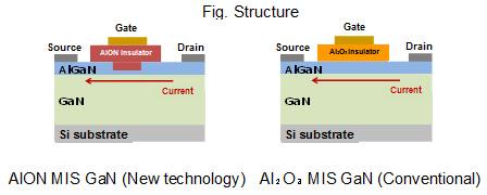
The use of a novel gate insulator of aluminum oxynitride (AlON, in which electrons are not easily trapped) suppresses hysteresis (in which the relation between gate voltage and drain current varies when the gate voltage is enhanced or applied repeatedly). This leads to continuous stable operation with a gate voltage up to +10V (maximum) for high-speed switching.
The crystal growth technique enables the formation of a recessed gate structure without process damage, making it possible to achieve a high drain current while maintaining normally-off operation (in which no current flows between the source and the drain when no voltage is applied to the gate).
The high current and high breakdown voltage were achieved by applying Panasonic’s proprietary technologies featuring process uniformity over large areas, which have been acquired through the mass production of GaN-on-Si power devices.
The new transistor is the result of collaborative research with assistant professor Takuji Hosoi and professor Heiji Watanabe of Osaka University, and professor Tamotsu Hashizume of Hokkaido University, partly supported by Cross-ministerial Strategic Innovation Promotion Program (SIP), ‘Next-Generation Power Electronics’ (funding agency: NEDO) of Council for Science, Technology and Innovation (CSTI) of the Cabinet Office, Government of Japan.
Panasonic GaN-on-Si power transistor


