


- News
2 January 2018
III-nitride resonant tunneling diodes at room temperature and below
Researchers in the USA have been studying III-nitride resonant tunneling diodes (RTDs) at room temperature and below [Jimy Encomendero et al, ‘New Tunneling Features in Polar III-Nitride Resonant Tunneling Diodes’, Phys. Rev. X, vol7, p041017, 2017].
The team from Cornell University, University of Notre Dame, and University of Utah, reports: “Resonant tunneling transport via the ground state and first excited state over a wide temperature window is demonstrated for the first time in III-nitride RTDs. These findings represent a significant step forward in resonant tunneling, intersubband-based physics, and III-nitride quantum devices.”
According to Huli Grace Xing, one of the authors from Cornell, room-temperature GaN RTDs have been sought after by the community for the past 20 years.
Theoretical work by the group suggests a sensitive dependence of performance on the built-in polarization fields due to charge density differences in the partial ionic bonding of aluminium nitride (AlN) and gallium nitride (GaN) layers used in the devices.
Resonant transport has been used in highly efficient injectors of electrons into the upper lasing level of terahertz (THz) quantum cascade lasers (QCLs), but applications have been hampered by the low temperatures needed to maintain quantum coherence in narrow-bandgap semiconductors such as the III-arsenide family.
Out of resonance conditions in RTDs since they result in decreasing currents with increasing bias – negative differential conductance – can be used to create high-frequency oscillators.
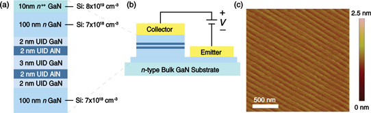
Figure 1: (a) Schematic of device structure and doping concentrations of GaN/AlN double-barrier heterostructure. (b) Cross-sectional schematic of fabricated resonant tunneling diode with collector and emitter metal contacts under forward bias. (c) Surface morphology of as-grown RTD heterostructure with root-mean-square roughness of ~0.146nm over a 2μmx2μm area.
GaN structures with double 2nm AlN barriers inserted (Figure 1) were grown on commercial c-plane n-GaN bulk substrates by molecular beam epitaxy (MBE). The dislocation density of the substrates was ~5x10⁴/cm2. The growth used metal-rich conditions at 700°C temperature with 200W-power nitrogen plasma. Such growth has been found to result in smooth surfaces. In particular, Ga was used as a surfactant during the AlN growth – Al is incorporated into the growth front in preference to Ga. The presence of Ga reduces the surface energy without getting incorporated. The Ga-rich conditions were used in a step-flow growth mode.
Scanning transmission electron microscopy (STEM) studies suggested that the barriers were 8 monolayers of AlN, and the GaN well was 11 monolayers. The fluctuation in barrier width was around 1 monolayer.
“Maintaining these conditions has proven to be critical for achieving atomically smooth interfaces and minimizing the formation of defects, which is crucial for resonant tunneling transport,” the team comments.
The smooth surface was aided by the fact that the thickness of the AlN barrier was below the critical thickness of 5-7nm for pseudomorphic films on GaN.
The RTD fabrication used titanium/aluminium/gold/nickel for the collector and titanium/aluminium/gold for the emitter contacts.
The devices exhibited a resonant peak in current and a region of negative differential conductance after the peak voltage. The peak is attributed to resonance of the energy of electron waves trapped between the barriers and the Fermi level of the biased region.
Sweeping back through the resonance results in the peak occurring at higher voltage due, it is thought, to some form of charge trapping. Different mesa areas give current scaling that suggests that sidewall leakage is not significant.
Further scans result in peaks at a higher voltage. The subsequent valley increases in current, giving a lower peak-to-valley current ratio (PVCR). The behavior stabilizes after a number of scans.
The team comments: “This behavior suggests the presence of defects in the AlN barriers in this sample that act as current leakage paths and degrade the energy filtering mechanism of the double-barrier heterostructure. It should be noted, however, that these leakage paths exhibit limited effects and do not prevent resonant tunneling transport of carriers across the active region at room temperature.”
Bias in the reverse polarity does not have a peak in the current-voltage (I-V) domain – rather there is firstly a low-injection-current region before a threshold voltage for higher current than in the forward direction. The team comments: “This asymmetric I-V is a direct consequence of the polarization electric fields present in the heterostructure, due to broken inversion symmetry of the uniaxial crystal.”
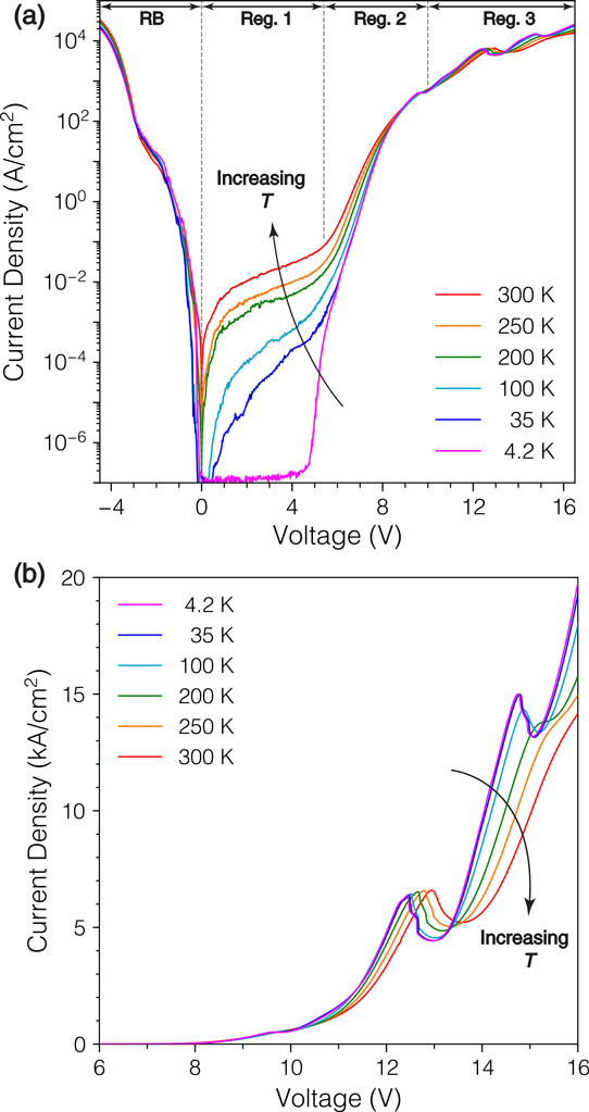
Figure 2: (a) Semilogarithmic I-V plot showing regions with different transport regimes as a function of temperature: under a reverse bias (RB), the current exhibits weak temperature dependence. By contrast, forward-bias region 1 shows strong temperature dependence attributed mainly to thermionic electrons. Region 2 presents a weak dependence on temperature due to enhancement of tunneling current component. Transport within region 3 is mainly due to resonant tunneling of carriers. (b) Forward I-V curves at different temperatures showing repeatable room-temperature resonant peak and higher-order resonance for temperatures below 200K.
Decreasing the temperature to 4.2K, the first resonance peak shifts to lower voltage and a second emerges, attributable to the resonant tunneling transport from the first excited state in the well between the barriers (Figure 2).
The researchers explain the asymmetric current-voltage behavior as resulting from the built-in polarization fields. The team has further analyzed the reverse-bias threshold behavior: “if we consider a set of polar RTDs with different barrier thicknesses, the polarization discontinuity will be given by half the slope of the threshold voltage versus barrier thickness, assuming symmetric double-barrier heterostructures.”
The polarization field was found to be 11.0MV/cm for AlN pseudomorphically strained on GaN, compatible with theoretical and experimental values. For example, a value of 10.9MV/cm has been extracted from experiments on AlN/GaN high-electron-mobility transistors.
Further analysis suggests that thinning the AlN barrier to 1nm could increase the resonant tunneling current by two orders of magnitude. “This trend is experimentally verified since RTDs featuring AlN barriers of 1.5nm and 2.4nm drive resonant currents of ~2.5x10²A/cm2 and ~2.6x10⁴A/cm2, respectively,” the team reports.
Devices with larger PVCR are expected from lowered MBE growth rates to enhance adatom mobility, reducing defect formation and creating atomically smooth interfaces for decreased carrier scattering. The built-in polarization fields can be avoided or reduced with non-polar or semi-polar substrates.
Resonant tunneling diodes GaN AlN MBE
https://doi.org/10.1103/PhysRevX.7.041017
The author Mike Cooke is a freelance technology journalist who has worked in the semiconductor and advanced technology sectors since 1997.


