


- News
16 January 2018
‘First’ quasi-vertical gallium nitride trench MOSFET on six-inch silicon
École Polytechnique Fédérale de Lausanne (EPFL) in Switzerland claims the first gallium nitride (GaN) quasi-vertical trench gate metal-oxide-semiconductor field-effect transistors (MOSFETs) on six-inch silicon (Si) substrates with 645V off-state breakdown [Chao Liu et al, IEEE Electron Device Letters, vol39, p71, 2018].
The researchers hope that combining compact vertical-structure GaN MOSFETs with silicon substrates will reduce costs for the emerging power electronics technology. Up to now, vertical GaN power devices have usually been produced on ultra-expensive bulk or free-standing GaN substrates, since reducing threading dislocations is imperative for low current leakage and for avoiding breakdown in the off-state. Threading dislocations arise from the large lattice and thermal expansion mismatch between silicon and GaN.
The researchers grew an n-p-n heterostructure on six-inch (111) silicon by metal-organic chemical vapor deposition (MOCVD). The structure consisted of a 1.1μm AlN buffer, 1μm of n+-GaN, a 4μm n--GaN drift layer, 350nm of p-GaN, a 200nm n-GaN layer, and 20nm of n+-GaN. The buffer used an optimized process, with particular focus on nucleation on silicon, to achieve a low-threading-dislocation-density, high-quality aluminium nitride layer. The subsequent GaN layers were grown without relaxation of compressive stress to compensate the tensile stress that arose during cooling after deposition.
Lateral mobility measurements on the drift layer gave a value of 720cm2/V-s. The team comments: “To the best of our knowledge, this is the highest electron mobility in vertical GaN on Si.”
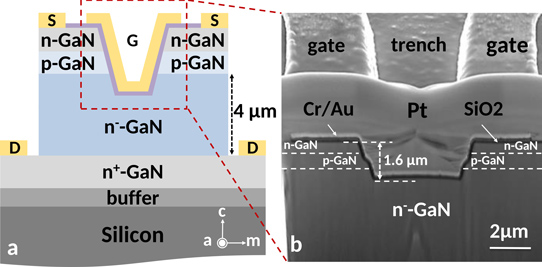
Figure 1: Cross-sectional (a) schematic, and (b) SEM image of fabricated quasi-vertical trench gate MOSFETs on Si substrate.
Transistor fabrication (Figure 1) involved dry etching 1.6μm-deep trenches, tetra methyl ammonium hydroxide (TMAH) wet etch to repair sidewall damage, rapid thermal annealing (RTA) to activate the p-type magnesium doping, atomic layer deposition (ALD) of 100nm silicon dioxide gate dielectric, contact hole etch, chromium/gold source-gate deposition, 5μm mesa etch, and chromium/gold drain deposition.
The on/off current ratio of the device was more than 108, while off-state leakage was less than 10-8kA/cm2. Gate leakage was 1.2x10⁻⁹kA/cm2 at 0V gate potential, rising to 2.5x10⁻⁶ at 15V. The team believes this can be reduced by trench and gate dielectric optimization.
The measured threshold of +6.3V confirmed normally-off operation. The researchers say that the high threshold “is preferable for high-power applications to guarantee a safe operation and better noise immunity.” The peak transconductance was269S/cm2.
With the gate and drain at 12V and 11V, respectively, the on-state current was 1.3kA/cm2 with a specific on-resistance of 6.8mΩ-cm2/
Hard breakdown of the 0V gate off-state occurred at 645V. The gate current was below 10-5kA/cm2 at breakdown. The team comments: “The observed breakdown was destructive and mainly happened at the mesa edges. By introducing field-plates and edge-termination technologies to these devices, the electric field at the junction edge could be reduced, which would further enhance their breakdown voltage. However, the performance observed even without edge termination is quite remarkable, which reveals the enormous potential for GaN-on-Si vertical transistors.”
Two-terminal circular n-p-n test structures had a similar breakdown at 679V. The similarity of the leakage current magnitude through different diameter structures indicate that the leakage flows mainly through the heterostructure rather than the etched sidewalls, according to the researchers.
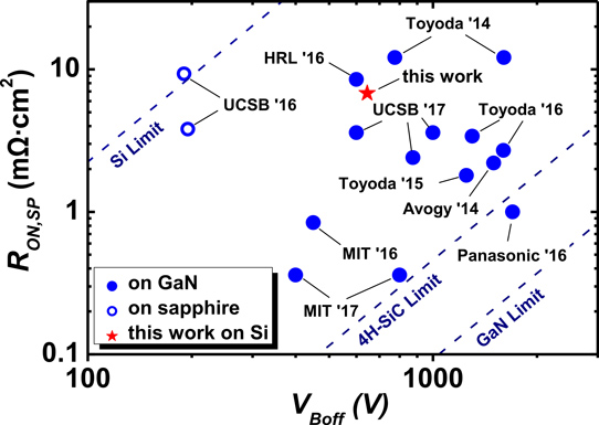
Figure 2: RON,SP versus VBoff benchmarks of vertical trench gate MOSFETs on silicon substrates with state-of-the-art enhancement-mode (normally-off) vertical transistors on sapphire and GaN substrates.
Combining the breakdown voltage (VBoff) with the specific on-resistance (RON,SP) gives a Baliga figure of merit (VBoff2/RON,SP) of 61MW/cm2. This improves on what has been achieved on sapphire (Figure 2).
The team believes that better results could be forthcoming from enhancing the TMAH wet etch of the sidewalls, adding field plates and edge-termination, and removing the silicon substrate to give fully vertical devices.
GaN MOSFET Silicon substrate MOCVD
https://doi.org/10.1109/LED.2017.2779445
The author Mike Cooke is a freelance technology journalist who has worked in the semiconductor and advanced technology sectors since 1997.


