


- News
19 January 2018
Fudan University develops optically pumped all-silicon laser
© Semiconductor Today Magazine / Juno PublishiPicture: Disco’s DAL7440 KABRA laser saw.
Silicon lasers are key to achieving integrated silicon photonics but, due to its indirect bandgap, the optical gains in silicon are lower than those of direct-bandgap III-V compound semiconductors by one or two orders of magnitude. Although the fabrication of matured III-V lasers on silicon substrates has been proposed to circumvent this problem, the development of an all-silicon laser is still highly desired for integrated silicon photonics, due to its better compatibility with state-of-the-art silicon techniques.
Recently, a joint research team led by professor X. Wu, professor M. Lu and associate professor S.-Y. Zhang at Fudan University developed what is claimed to be the first all-silicon laser using silicon nanocrystals with high optical gain (Dong-Chen Wang et al, ‘An all-silicon laser based on silicon nanocrystals with high optical gains’, Science Bulletin, 5 January 2018).
First, they enhanced the silicon emission intensity greatly by developing a film growth technique for high-density silicon nanocrystals (Physica E, 89, 57-60(2017)). Then they developed a high-pressure low-temperature passivation approach, which contributed to the full saturation of dangling bonds, leading to increased optical gains that were comparable to those achieved by gallium arsenide (GaAs) and indium phosphide (InP).
On this basis, they designed and fabricated distributed feedback (DFB) resonance cavities and successfully achieved optically pumped all-silicon DFB lasers. The optically pumped all-silicon laser also paves the way towards the realization of electrically pumped all-silicon laser.
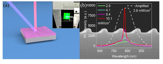
Graphic: (a) Schematic image of DFB silicon laser; inset: photograph of fabricated DFB device. (b) Emission spectra of the silicon laser as a function of pump power; background: cross-sectional SEM image of DFB structure.
It was found that the optical gain of silicon nanocrystals was constantly enhanced as the passivation proceeded and eventually reached the value comparable to those of GaAs and InP. Lasing characteristics - the threshold effect, the polarization dependence, the significant spectral narrowing and small spread of divergence angle of stimulated emission - were fulfilled, suggesting the realization of an optically pumped all-silicon laser.
The full-width-at-half-maximum (FWHM) of the emission peak was narrowed from ~120nm to 7nm when the laser was pumped above threshold.
The lasers also showed reliable repeatability. The lasing peaks of the four additional samples made under similar fabrication conditions were within the spectral range 760-770nm. The variation in the lasing peak was due to the slight difference in effective refractive indices.
The program is supported by the National Natural Science Foundation of China (51472051, 61275178, 61378080, 61705042) and Shanghai Sailing Program (16YF1400700).
Laser diodes Silicon substrate silicon photonics
https://www.sciencedirect.com/science/article/pii/S2095927318300069


