


- News
31 January 2018
Stacking III-nitride laser diodes with tunnel junction connections
Hamamatsu Photonics K.K. in Japan says that it has demonstrated room-temperature operation of nitride-based stacked laser diodes (LDs) with tunnel junctions for the first time [Satoru Okawara et al, Appl. Phys. Express, vol11, p012701, 2018].
The researchers hope that multiple-stack nitride-based laser diodes will lead to high-peak-power applications such as long-range light detection and ranging (LiDAR) for automotive vehicles and industry. In particular, the team points to the much higher maximum permissible exposure (MPE) for the human eye of pulsed near-ultraviolet light from III-nitride emitters, compared with the near-infrared produced by other III-V compound semiconductor systems. The stacking of laser diodes should reduce peak operating current – high-peak-current devices are difficult to pulse due to high reverse voltages from inductance effects.
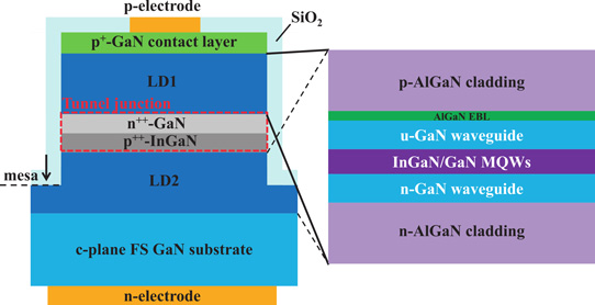
Figure 1: Schematic device structure of two-stack laser diode with tunnel junction.
The material structure was grown by metal-organic vapor phase epitaxy on free-standing GaN (Figure 1). Optically the two laser diodes were designed to ‘fully confine’ the ~395nm-wavelength light fields in the two guided region without crosstalk. The laser diode sections consisted of 1000nm n-aluminium gallium nitride Al0.07Ga0.93N cladding, a 200nm n-GaN waveguide, a 2-period indium gallium nitride (In0.06Ga0.94N)/GaN multiple quantum well, a 200nm undoped GaN waveguide, and 400nm of p- Al0.07Ga0.93N cladding.
The tunnel junction connecting the devices was 5nm p++-InGaN and 30nm n++-GaN. The researchers comment: “The thicknesses, indium composition, and doping concentrations of the tunnel junction were optimized to lower the voltage drop at the tunnel junction and to suppress the generation of hexagonal thermal pits originating from the tunnel junction layer, because the hexagonal pits generally act as current leakage paths, deteriorating the laser diode performance.”
Twin laser devices were fabricated by etching down to the n-cladding of the lower laser diode; activation of the p-type layers; deposition of nickel/gold p-electrodes, silicon dioxide insulation and titanium/gold n-electrodes; and cleaving and passivating mirror facets. The p-activation aimed at removal of hydrogen – in the lower layers this entailed lateral diffusion. The mirror passivation was aluminium oxide. The gain-guided broad-area cavity was 70μmx1000μm. The devices were assembled p-side up into TO-9 packages.
Current-voltage studies of the double laser diode gave a series resistance of 45Ω at 50mA injection, compared with 3.5Ω for a single emitter. The corresponding turn-on voltages were 6V and 3V. The team mainly blames the high resistance on insufficient removal of hydrogen from the buried p-type layers.
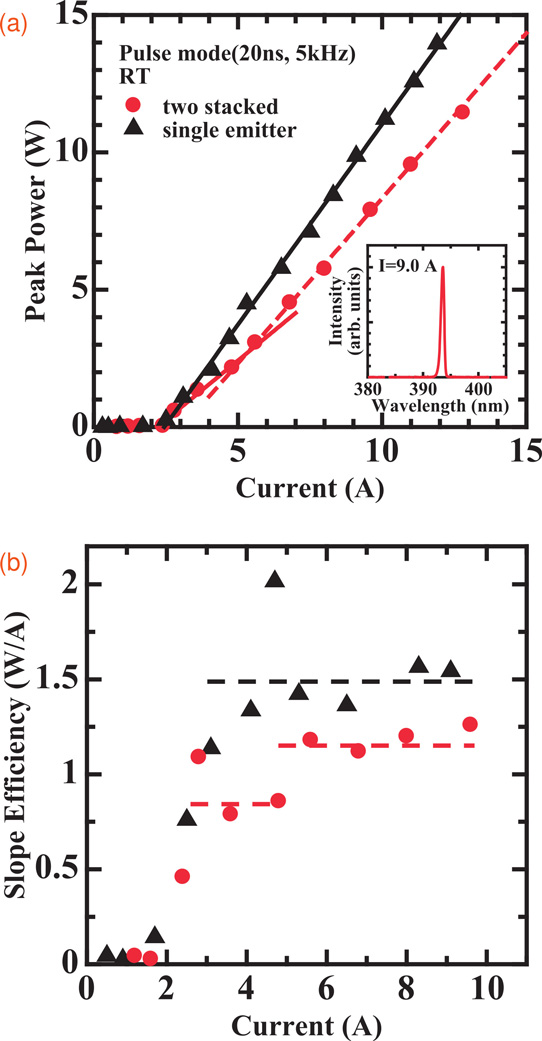
Figure 2: (a) Light output power and (b) slope efficiency versus current of two-stack (red circles) and single-emitter (black triangles) laser diodes under pulsed operation. Inset: optical spectrum of two-stack laser diode with emission wavelength of 394nm.
In 5kHz 20ns-pulsed-mode operation (Figure 2), the stacked laser diodes output 394nm wavelength at 9A injection. The radiation from the two laser diode components could not be distinguished. The comparison single-emitter had a linear 1.5W/A laser slope up 10W output power.
For the double laser diode, there were two laser thresholds at 2.4A and 5.2A. The slope after the first threshold was 0.8W/A and, after the second, 1.1W/A. The team reports: “The slope efficiencies of the stacked laser diode were lower than that of the single-emitter laser diode because of the non-optimized mirror facet coating of the stacked laser diode.” They also associate the first threshold with the upper laser diode (0.8W/A slope efficiency) and the second with the lower device (0.3W/A).
Further problems could arise from degradation of the InGaN layers in the bottom laser diode during subsequent high-temperature growth steps of the upper laser diode. “In addition, the p-dopant diffusing from the p++-InGaN layer of the tunnel junction into the cladding layer of LD2 might increase the optical absorption loss for lasing,” the researchers add.
Stacked laser diodes LiDAR InGaN AlGaN
https://doi.org/10.7567/APEX.11.012701
The author Mike Cooke is a freelance technology journalist who has worked in the semiconductor and advanced technology sectors since 1997.


