


- News
10 January 2018
Integrating indium gallium arsenide transistor and III-V laser on silicon
Researchers based in Singapore and the USA have integrated indium gallium arsenide (InGaAs) transistors with aluminium gallium arsenide (AlGaAs) laser diodes (LDs) using molecular beam epitaxy (MBE) on silicon substrates [Annie Kumar et al, Optics Express, vol25, p31853, 2017].
The team from National University of Singapore, the Singapore-MIT Alliance for Research and Technology-Low Energy Electronic Systems, Nanyang Technological University in Singapore and Massachusetts Institute of Technology (MIT) in the USA are working towards low-cost, low-power, high-speed optoelectronic integrated circuits (OEICs). The same grouping of institutions reported in March 2017 transistor/LD integration on germanium substrate [www.semiconductor-today.com/news_items/2017/mar/nus_290317.shtml].
In their latest work, the Si (100) substrate was offcut 6°C in the (110) direction. The germanium (Ge) part of the buffer was grown in a three-step process, reducing the intentional doping to zero, which achieved a threading dislocation density of less than 5x10⁶/cm6. The III-V layers were grown after 650°C annealing under ultra-high vacuum aimed at creating Ge double atomic steps on the surface of the buffer layer, designed to avoid anti-phase boundaries (APB).
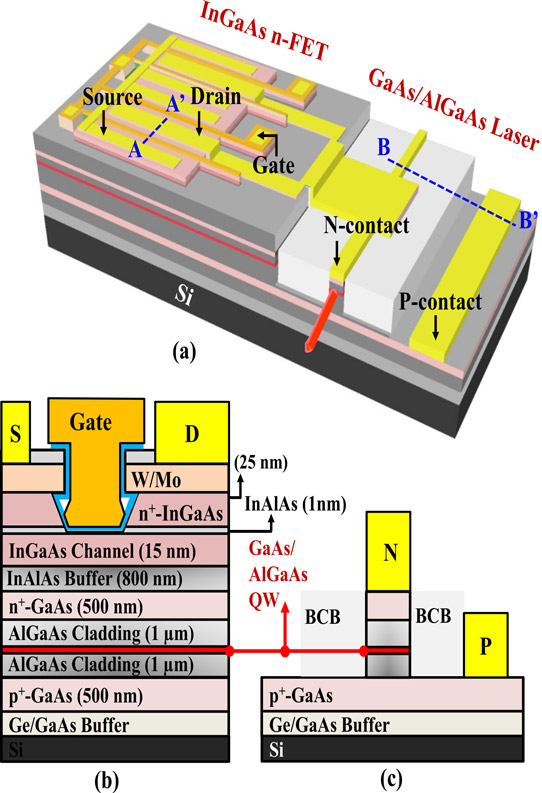
Figure 1: (a) Three-dimensional schematic of monolithic integration of self-aligned InGaAs MOSFETs and GaAs/AlGaAs QW laser on Si substrate. Drain of multi-finger transistor is connected to laser’s n-contact. (b) Cross-sectional schematic of InGaAs metal-oxide-semiconductor field-effect transistors (MOSFETs) with detailed layer structure and thicknesses along line AA’ in (a). (c) Cross-sectional schematic of GaAs/AlGaAs QW laser along line BB’ of (a).
The III-V growth was nucleated with 20 monolayers of GaAs grown at 300°C in low-temperature migration-enhanced epitaxy (MEE) to give good surface quality and to reduce APB-related defects. Further growth of the III-V heterostructure was carried out at 580°C. The laser active region consisted of a 5nm GaAs single quantum well with Al0.3Ga0.7As barriers in graded-index separate-confinement heterostructures that varied in Al content between 30% and 60%, bridging across to the Al0.6Ga0.4As crystal lattice of the cladding layers. Photoluminescence from the laser structure gave a peak wavelength of 788nm.
The transition to the transistor layers was achieved with an InAlAs buffer with indium content increasing from 0.1 to 0.52, giving a lattice matching with In0.53Ga0.47As (the favored material for high speed transistors).
Device fabrication produced metal-first self-aligned gate transistors followed by laser diodes. The n+ raised source drain contact metals were sputtered molybdenum and tungsten. Atomic layer deposition (ALD) formed the high-k insulator part of the gate stack with 1.5nm aluminium oxide and 5.5nm hafnium dioxide. Molybdenum and tungsten were also used for the gate electrode. Mesa etching of part of the InAlAs buffer between the transistor and laser layers and plasma-enhanced chemical vapor deposition (PECVD) of silicon dioxide passivation completed the transistor part of the fabrication.
Dry and wet etch opened up regions for laser fabrication. Further etching formed the laser structure. Smooth, vertical mirror facets were formed using 250°C plasma etch and PECVD silicon dioxide hard mask. The p-contact metals were titanium/gold. The structure was then planarized with benzocyclobutene (BCB). The top of the laser diode was exposed and annealed gold/germanium/nickel used as the n-contact stack.
Wiring connecting the transistor and laser were created by a metal lift-off process. The device wafer was finally thinned and diced. The fabrication process had a maximum temperature of 400°C. The researchers comment: “The low thermal budget of the overall process helped to maintain the high quality of the QW.”
One of the transistors with a 420nm-long channel achieved an on/off current ratio of six orders of magnitude with both 50mV and 500mV drain biases. With 50mV drain the minimum subthreshold swing (S) was 82mV/decade. The threshold was at 50mV gate potential. The drive current was 455μA/μm with the gate 0.95V over threshold and 1V drain bias. The peak transconductance with 0.5V drain was 443μS/μm.
Statistical work on a range of transistors showed an improvement in subthreshold after laser diode fabrication, with the mean falling from 107mV/decade to 81mV/decade. The researchers comment: “This improvement in S is attributed to post metal anneal (PMA) during SiO2 deposition at 350°C which leads to reduction of interface traps at high-k/InGaAs interface”.
The laser diode fabrication also improves threshold uniformity and puts it at a positive rather than negative value, due to a reduction in fixed positive charge in the high-k gate oxide stack, according to the researchers.
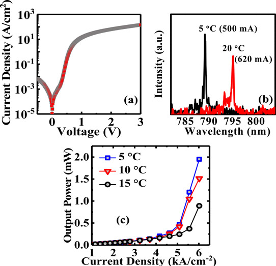
Figure 2: (a) Current density-voltage curve of GaAs/AlGaAs QW laser diode showing on/off current ratio of more than four orders of magnitude. (b) Lasing spectra at 5°C and 20°C at single-mode lasing currents of 500mA and 620mA, respectively. (c) Output power as function of current density for 540μmx20μm-wide laser at various operating temperatures.
As for the laser diode performance, under pulsed operation single-mode lasing at 5°C and 20°C had full-widths at half-maximum (FWHMs) of 0.3nm and 0.35nm, respectively. The respective wavelengths were 789nm at 500mA current injection and 795nm at 620mA. The wavelength shift corresponds to the bandgap energy temperature shift of GaAs. The team comments: “Although the FWHM of around 0.3nm is wider as compared to lasers grown on native III-V substrate, it is less or comparable to III-V lasers epitaxially grown on Si substrate.”
The threshold current density for a 540μmx20μm laser diode was 4.9kA/cm6 at 5°C, higher than the team’s previous III-V laser diodes on bulk germanium.
A combined circuit of transistor and laser diode with 2V operating voltage had a through current of the order of 15mA, much less than the 600mA needed for laser output. The researchers suggest that quantum dot devices could lower the laser threshold sufficiently for transistor modulation purposes.
The researchers point out another problem of the proof of concept in that the silicon substrate is not transparent to the produced light. Transparency would require narrower bandgaps for the active region as provided by InGaAs. The team comments: “As compared to the GaAs/AlGaAs system, using the InxGa{1-xAs/GaAs system with a higher Indium composition involves a higher lattice mismatch with respect to silicon and the challenge of growing such materials with low defectivity for laser fabrication on silicon need to be addressed.”
InGaAs InGaAs transistors AlGaAs AlGaAs laser diodes MBE Silicon substrates
https://doi.org/10.1364/OE.25.031853
The author Mike Cooke is a freelance technology journalist who has worked in the semiconductor and advanced technology sectors since 1997.


