


- News
30 January 2018
Boosting indium gallium nitride LEDs on silicon with tensile stress
South China University of Technology has improved the performance of indium gallium nitride (InGaN) light-emitting diodes (LEDs) on silicon through increasing tensile stress in the photon-generating active region [Zhiting Lin et al, J. Appl. Phys., vol122, p204503, 2017]. Although stress engineering has been a critical factor in enabling III-nitrides to be grown on low-cost silicon, overcoming 16.9% lattice and 54% thermal mismatching, the researchers note that the effect of stress on “performance of LEDs by modifying the band structure and the carrier recombination process, seems to be neglected”.
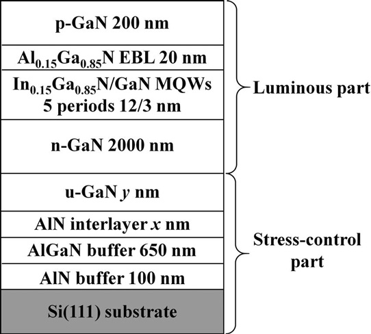
Figure 1: Experimental LED structure.
LED material (Figure 1) was grown by metal-organic chemical vapor deposition (MOCVD) on (111) silicon. The stress state of the ‘luminous’ multiple quantum well (MQW) upper layers was controlled by varying the thickness of underlying undoped u-GaN and AlN layers (Table 1). The crystalline quality was assessed through full-width at half maximum (FWHM) measurements of peaks in x-ray rocking curves (XRCs) and microscopic inspection of cracks in the surface. Raman spectroscopy was used to derive the stress state of the MQW. Increasing GaN thickness and removal of the AlN interlayer increased tensile stress. However, if taken too far, cracks appear.
Table 1: Material and photoelectric properties of LEDs A to D, including thicknesses of AlN interlayer and u-GaN that provide stress variation.
| Sample | LED A | LED B | LED C | LED D |
| AlN interlayer (nm) | 20 | 20 | 0 | 0 |
| u-GaN (nm) | 400 | 800 | 800 | 1200 |
| GaN(0002) XRC FWHM (arc sec) | 368 | 355 | 350 | 352 |
| GaN(10-12) XRC FWHM (arc sec) | 434 | 433 | 430 | 435 |
| Stress (GPa) | -0.63 | 0.13 | 1.03 | 0.71 |
| Crack density (/mm2) | 0 | 0 | 0 | 2.45 |
| LOP at 35A/cm2 (mW) | 442 | 510 | 528 | 482 |
| Vf at 35A/cm2 (V) | 3.11 | 3.08 | 3.05 | 3.17 |
| WPE at 70A/cm2 | 32.2% | 38.3% | 40.0% | 34.1% |
The material was fabricated into 1mmx1mm LED chips. The light output power (LOP) of LED C with most tensile stress was 19.4% greater than that of LED A (Figure 2). The 35A/cm2 forward voltage (Vf) for LED C was also lowest, giving the least power input at the given current injection and further boosting wall-plug efficiency (WPE). At 70A/cm2, the WPE droop was 36.5% for LED C. This droop was the smallest among the devices. The researchers say that the LOP of 528mW at 35A/cm2 for LED C is greater than the ~508mW of devices on silicon reported by other groups.
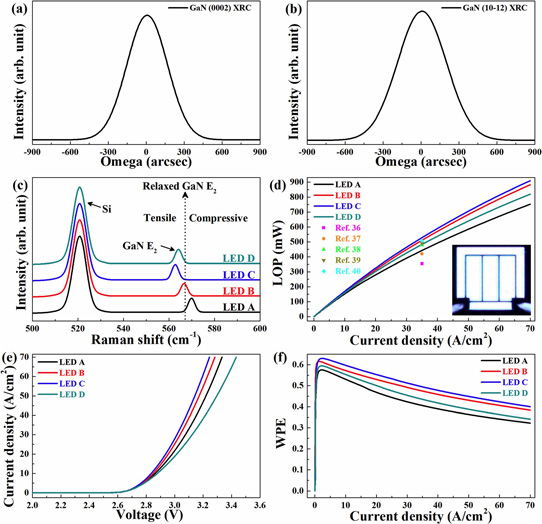
Figure 2: (a) GaN(0002) and (b) GaN(10-12) XRCs for LED C, (c) Raman spectra of LEDs A to D. (d) Experimental light output power versus current density, (e) current density versus voltage, and (f) wall-plug efficiency versus current density for LEDs A to D.
Despite its higher tensile stress, the performance of LED D was worse than that of LED B. “The cracks of LED D may induce some connotative damage during the fabrication of LED chips, resulting in the degradation of the light output power and the increment of electric resistance,” the team comments.
Simulations suggested that going from compressive stress of -3GPa to tensile stress of +5GPa should improve luminous output and generally reduce forward voltage for an injection current density of 35A/cm2. Actually, the lowering of forward voltage only continued up to +4GPa. Increasing the tensile stress up to +8GPa impaired the projected LED performance beyond that at -3GPa compression. On the other hand, at low current injection the +8GPa model gave the best performance.
Charge polarization due to the partial ionic nature of the III-N bonds gives rise to sheet charges at heterointerfaces and hence electric fields in the structures. The effect is altered by different stress states and can impact band structure, carrier recombination, and carrier concentration in MQWs.
The researchers comment: “It is demonstrated by simulation that tensile stress in the underlying n-GaN alleviates the negative effect from polarization electric fields on multiple quantum wells, but an excessively large tensile stress severely bends the band profile of the electron blocking layer, resulting in carrier loss and large electric resistance.”
https://doi.org/10.1063/1.4993985
The author Mike Cooke is a freelance technology journalist who has worked in the semiconductor and advanced technology sectors since 1997.


