


- News
23 January 2018
Reducing dislocations in gallium arsenide on silicon templates
University of California Santa Barbara (UCSB) in the USA has been working to optimize gallium arsenide (GaAs) molecular beam epitaxy (MBE) on gallium phosphide on silicon (GaP/Si) [Daehwan Jung et al, J. Appl. Phys., vol122, p225703, 2017]. Normally, growth of GaAs on Si uses off-axis substrates in efforts to avoid anti-phase domains. On-axis silicon is preferred for compatibility with CMOS processing foundries. The lattice mismatch between GaAs and Si is ~4%, leading to dislocations.
The researchers managed to reduce threading dislocation densities (TDDs) to 7.2x10⁶/cm2, a factor of 40 lower than for an unoptimized process. They comment: “We believe that these high-quality GaAs buffer layers with low TDDs and smooth surfaces will serve as versatile templates for high-performance Si-based optoelectronic devices, including lasers and photodetectors as well as a myriad of photonic integrated circuits made from these devices.”
The researchers used a commercial 300mm GaP/Si (001) template from NAsPIII/V GmbH. The estimated unintentional miscut of the template was potentially only 0.1-0.2°. The silicon wafer was subjected to a special pre-epitaxial heat treatment designed to terminate anti-phase domains in the 45nm GaP layer.
The wafer was cut up into small pieces and put on molybdenum adapting plates in the Veeco MBE chamber. After oxide desorption, the growth began with 100nm GaAs at 400-550°C. The temperature was then raised to 600°C for 3μm GaAs layer growth.
Electron channeling contrast imaging (ECCI) measurements gave a threading dislocation density (TDD) of ~2.8x10⁸/cm2 averaged over a 1800μm2 area on a reference unoptimized GaAs/GaP/Si sample, which was consistent with results from more traditional plan-view transmission electron microscopy (TEM). ECCI allows dislocation density assessments over larger areas, reducing uncertainties. Root-mean-square (RMS) roughness of the reference was 7.8nm, according to atomic force microscopy (AFM) on 10μmx10μm fields.
Various optimizations were applied to the growth process: in-situ thermal cycle annealing, dislocation filter layers, and altering the growth temperature of the low-temperature GaAs layer.
The annealing consisted of 500°C low-temperature GaAs, 1.5μm high-temperature GaAs, 4x thermal cycling between 700°C and 320°C, and 1.5μm more high-temperature GaAs. ECCI measurements gave a TDD of 5.5x10⁷/cm2. RMS roughness was 4.8nm. The team believes that the dislocations are removed by gliding and misfits fusing or annihilating.
A variety of dislocation filter layers were tested. The best involved 10 periods of 10nm indium gallium arsenide (In0.1Ga0.9As) and 10nm GaAs applied after thermal cycle annealing, giving 7.2x10⁶/cm2 TDD and 2.9nm RMS roughness. The 200nm filter was capped with 1.3μm GaAs. The InGaAs was applied at 500°C. Somewhat lower TDDs of 1.2-1.4x10⁶/cm2 have been achieved with metal-organic chemical vapor deposition (MOCVD) on 4-6° offcut substrates. Also, higher annealing temperatures can be reached in MOCVD chambers.
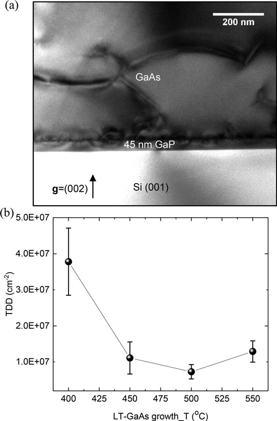
Figure 1: (a) Cross-sectional bright-field transmission electron micrograph of GaAs on GaP/Si. (b) TDD versus low-temperature-GaAs growth temperatures.
Variation of the low-temperature GaAs nucleation layer found that 500°C was optimal for a structure grown with thermal cycle annealing and InGaAs/GaAs dislocation filtering (Figure 1). Also adding extra dislocation filter layers (DFLs) increased the TDD level, while paradoxically decreasing roughness. The team explains: “We believe that adding more sets of DFLs nucleated more dislocations to relax the upper InGaAs/GaAs DFLs rather than recycling the pre-existing TDs.”
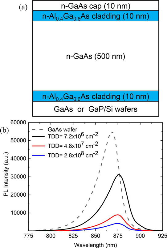
Figure 2: (a) Schematic of GaAs/AlGaAs PL structure. (b) Room-temperature PL spectra of GaAs PL samples grown on native GaAs, and three different GaAs/GaP/Si templates.
Photoluminescence (PL) measurements were made on GaAs in aluminium gallium arsenide (AlGaAs) cladding structures grown on three GaAs/GaP/Si templates with TDDs varying between 2.8x10⁸/cm2 and 7.2x10⁶/cm2 (Figure 2). The researchers report: “It is noted that the integrated PL intensity from the optimized GaAs buffer layer is 7 times larger than the reference sample (TDD=2.8x10⁸/cm2). Compared with the GaAs layer grown on a native GaAs wafer, the optimized sample shows only ~40% reduction in the PL intensity at room temperature.”
GaAs MBE GaP Silicon substrate NAsPIII/V GmbH
https://doi.org/10.1063/1.5001360
The author Mike Cooke is a freelance technology journalist who has worked in the semiconductor and advanced technology sectors since 1997.


