


- News
10 July 2018
3D-Micromac unveils microPREP 2.0 laser-based high-volume sample prep system for failure analysis
© Semiconductor Today Magazine / Juno PublishiPicture: Disco’s DAL7440 KABRA laser saw.
In booth #1645 (South Hall) at SEMICON West 2018 in San Francisco (10-12 July), 3D-Micromac AG of Chemnitz, Germany (which provides laser micromachining and roll-to-roll laser systems for the semiconductor, photovoltaic, medical device and electronics markets) has launched the microPREP 2.0 laser ablation system for high-volume sample preparation of metals, semiconductors, ceramics and compound materials for microstructure diagnostics and failure analysis (FA).
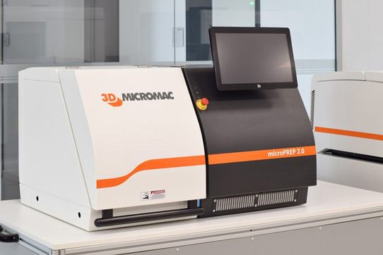
Picture: The microPREP 2.0 laser ablation system.
Built on a highly flexible platform with a small table-top footprint, the microPREP 2.0 allows for easy integration into FA workflows, says the firm. Developed jointly with Fraunhofer Institute for Microstructure of Materials and Systems (IMWS) in Halle (Saale), Germany, the microPREP 2.0 complements existing approaches to sample preparation such as focused ion beam (FIB) micromachining, offering up to 10,000 times higher ablation rates and therefore an order-of-magnitude lower cost of ownership (CoO) compared with FIB, it is reckoned. As what is claimed to be the first stand-alone, ultrashort pulsed laser-based tool for sample preparation, the microPREP 2.0 has additional unique capabilities such as enabling large-area and 3D-shape sampling to allow for more comprehensive testing of complex structures.
Cutting and preparing samples from semiconductor wafers, dies and packages for microstructure diagnostics and FA is an essential but time-consuming and costly step. The primary method of sample preparation used in semiconductor and electronics manufacturing currently is FIB micromachining, which can take several hours to prepare a typical sample. FIB only allows for very small sample sizes, and FIB time is wasted by ‘digging’ excavations needed for cross-sectional imaging in a scanning electron microscope or making a TEM lamella. Reaching larger depths or widths is severely restricted by the limited ablation rate.
3D-Micromac says that its microPREP 2.0 significantly accelerates these critical steps. By off-loading the vast majority of sample prep work from the FIB tool and relegating FIB to final polishing or replacing it completely depending on application, microPREP 2.0 reduces time to final sample to less than 1 hour in many cases, it is reckoned.
“This award-winning tool brings unprecedented flexibility into sample prep. We at Fraunhofer IMWS are facing the need for targeted, artifact-free and most reliable preparation workflows to be able to serve our industry customers with cutting-edge microstructure diagnostics,” says Thomas Höche of Fraunhofer IMWS. “Made for diverse techniques like SEM inspection of advanced-packaging devices, x-ray microscopy, atom probe tomography and micro mechanics, microPREP was developed jointly with 3D-Micromac to close gaps in preparation workflows,” he adds.
Last month, 3D-Micromac and Fraunhofer IMWS received the TUV SUD Innovation Award for their collaboration on the development of microPREP 2.0. The annual prize honors cooperation between small- and medium-size enterprises and research institutions. It is administered by TUV SUD, a technical service corporation serving the industry, mobility and certification segments.
Key benefits of microPREP 2.0 are cited as:
- much higher ablation rate compared with FIB (by several orders of magnitude);
- high degree of automation due to a recipe-based, ergonomic user interface;
- extremely high energy densities can be focused in very small areas (allowing for operation in the multi-photon absorption regime needed to machine at-wavelength-transparent materials and enabling stable process windows);
- virtually no structural damage from local heating due to the platform’s very short pulse lengths (pico-second range);
- providing larger-sized samples with micron-level precision — enabling multi-site FA on whole chip or package areas in a much shorter period of time and a multitude of workflows delivering samples for various FA techniques;
- enables the creation of samples with complicated/3D shapes to enable more comprehensive analysis of certain structures, such as through-silicon vias (TSVs) or even complete systems-in-package (SiP); and
- laser processing without elemental contamination.
3D-Micromac says that microPREP 2.0 can be used for a variety of sample preparation applications, including: in-plane geometries and bulk samples; cross-sections; box milling (e.g. for diagnostics of electrical connections and 3D chip-level structures); and full line cut (for complex investigations of complete devices). Samples can be moved between microPREP 2.0 and FA tools using the same pin stubs and holders, which provides even greater ease of use and time savings.
“The growing complexity of microelectronics manufacturing is driving the need for faster, more reliable and cost-effective, and artifact-free sample preparation techniques at the micron scale,” says chief sales officer Jan Klinger. “Building on our extensive expertise in laser micromachining, 3D-Micromac can now offer an optimal sample preparation solution for this market,” he adds. “By off-loading the coarse and time-consuming task of sample preparation to a simple and fast support tool, microPREP frees up our customers’ time to focus their efforts on fab-critical issues like trouble-shooting process and yield problems.”


