


- News
12 July 2018
Speeding oscillation of double heterojunction bipolar transistors
Researchers at ETH Zurich in Switzerland claim the fastest quaternary-base double heterojunction bipolar transistor (DHBT) reported to date with maximum oscillation (fMAX) greater than the cut-off (fT) frequency, grown by metal-organic chemical vapor deposition (MOCVD) [Wei Quan et al, IEEE Electron Device Letters, published online 21 June 2018].
The quaternary base consisted of graded gallium indium arsenide antimonide (GaInAsSb). Adding indium to GaAsSb improves electron transport properties such as mobility and sheet resistance. GaAsSb’s conduction band has two types of valley – one at zero wavevector (the Γ point) and one in the ‘L’ directions of the crystal structure. In GaAsSb, the L-valley is close in energy to the central Γ-valley. Electrons can be trapped in the L-valley, reducing performance.
The researchers comment: “Consideration of the DHBT higher bandstructure suggests the performance improvement mechanism is a reduction of the L-valley population in the GaInAsSb base and an associated easier collection into InP [indium phosphide].”
The team sees promise for the device in high-linearity high-efficiency amplification in sub-millimeter wavelength radio frequency integrated circuit applications.
MOCVD (Table 1) was carried out on 2-inch semi-insulating InP. Carbon (C) was used for p-doping of the base region, achieved through constant carbon tetrabromide precursor flux. The grading of the GaInAsSb composition resulted in variation of the uptake of carbon, decreasing with higher indium content, giving linear concentration grading between 3.1x10¹⁹/cm3 and 8.1x10¹⁹/cm3.
Table 1: Epitaxial layer structure.
| Emitter | Ga0.25In0.75As | Si: 3.8x10¹⁹/cm3 | 5nm |
| Emitter | Ga0.47In0.53As → Ga0.25In0.75As | Si: 3.8x10¹⁹/cm3 | 10nm |
| Emitter | Ga0.47In0.53As | Si: 3.8x10¹⁹/cm3 | 20nm |
| Emitter | InP | Si: 1.5x10¹⁹/cm3 | 130nm |
| Emitter | InP | Si: 2.5x10¹⁶/cm3 | 5nm |
| Emitter | Ga0.20In0.80P → InP | Si: 2.5x10¹⁶/cm3 | 10nm |
| Emitter | Ga0.20In0.80P | Si: 2.5x10¹⁶/cm3 | 5nm |
| Base | Ga0.83In0.17As0.62Sb0.38 → Ga0.94In0.06As0.70Sb0.30 | C: 3.1x10¹⁹/cm3 → 8.1x10¹⁹/cm3 | 20nm |
| Collector | InP | Si: 9.1x10¹⁶/cm3 | 125nm |
| Collector | InP | S: 2.8x10¹⁹/cm3 | 50nm |
| Collector | Ga0.47In0.53As | Si: 3.0x10¹⁹/cm3 | 20nm |
| Collector | InP | S: 2.8x10¹⁹/cm3 | 300nm |
| Substrate | InP | Semi-insulating | 350μm |
The device was designed with type-I alignment between the emitter and base and type-II alignment between the base and collector. The type-II alignment avoids blocking of electrons flowing into the collector. The alignment types I and II describe how the conduction and valence bands change at heterojunctions between different material compositions. In the type I alignments, the two bands change in opposite directions, while in type II the bands step in the same direction.
The DHBTs were fabricated in a process involving self-aligned triple mesas using the emitter and base contacts as etch masks. The emitter and base contacts consisted of titanium/platinum/gold and palladium/nickel/platinum/gold, respectively. The etching involved dry and wet processes. Atomic layer deposition (ALD) of aluminium oxide was used for passivation of emitter sidewalls and extrinsic base surfaces.
The collector mesa was produced using wet etching. Undercutting of the collector mesa reduced extrinsic base-collector capacitance. Probe pads were produced by evaporation of metal and a low-temperature Teflon-based etch-back and planarization process. Tefllon has a lower dielectric constant (1.9 versus 2.7) compared with more conventional benzocyclobutene (BCB) polymer, allowing higher-speed signal transmission and switching by reducing parasitic capacitance.
The researchers tested a device with 0.3μmx3.5μm emitter area (AE). The base and collector current idealities were 1.78 and 1.04, respectively. The peak common emitter current gain was 16. Plasma etch damage reduced the gain. Larger devices fabricated with just wet etching achieved gains up to 32. Common emitter breakdown occurred at 5.1V, when the collector current density was 1kA/cm2 (0.01mA/μm2). The offset voltage of 70mV is described as ‘very low’.
Radio-frequency measurements up to 50GHz gave extrapolated maximum oscillation (fMAX) and cut-off (fT) frequencies of 784GHz and 547GHz, respectively (Figure 1). The collector-emitter voltage bias-point (VCE) was 1.0V with the collector current (JC) at 9.1mA/μm2. Standard de-embedding gives 816GHz fMAX and 552GHz fT. Molecular beam epitaxy (MBE) GaInAsSb-base devices have achieved fT/fMAX performance of 670GHz/185GHz. MOCVD graded-base DHBTs have clocked up 513GHz/637GHz.
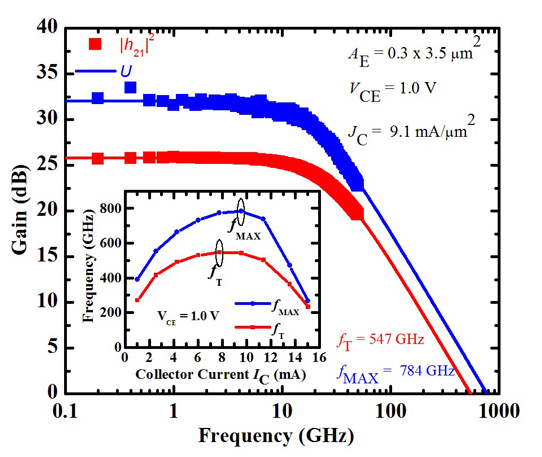
Figure 1: Short-circuit current gain (|h21|2) and Mason’s unilateral gain (U) measured between 0.2GHz and 50GHz. Inset: dependence of fT and fMAX on collector current at 1.0V VCE.
The team reports: “The total base resistance extracted from RF measurements amounts to RB = 25.3Ω5 with a contact contribution of 2.8Ω, corresponding to a base contact resistance of 0.31Ω-μm2. The fMAX is therefore limited by the base sheet resistance in the present devices.”
https://doi.org/10.1109/LED.2018.2849351
The author Mike Cooke is a freelance technology journalist who has worked in the semiconductor and advanced technology sectors since 1997.


