- News
12 July 2018
Imec demos hybrid FinFET-silicon photonics technology for ultra-low power optical I/O
© Semiconductor Today Magazine / Juno PublishiPicture: Disco’s DAL7440 KABRA laser saw.
At its Imec Technology Forum USA in San Francisco, nanoelectronics research centre imec of Leuven, Belgium announced that it has demonstrated ultra-low-power, high-bandwidth optical transceivers through hybrid integration of silicon photonics and FinFET CMOS technologies. With a dynamic power consumption of only 230fJ/bit and a footprint of just 0.025mm2, the 40Gb/s non-return-to-zero (NRZ) optical transceivers are said to represent a milestone in realizing ultra-dense, multi-Tb/s optical I/O solutions for next-generation high-performance computing applications.
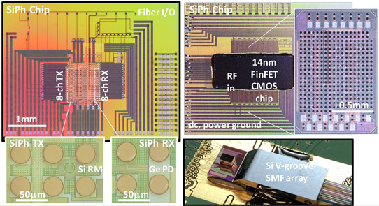
The exponentially growing demand for I/O bandwidth in data-center switches and high-performance computing nodes is driving the need for tight co-integration of optical interconnects with advanced CMOS logic, covering a wide range of interconnect distances (1m-500m+), says imec. In the presented work, a differential FinFET driver was co-designed with a silicon photonics ring modulator, and achieved 40Gb/s NRZ optical modulation at 154fJ/bit dynamic power consumption. The receiver included a FinFET trans-impedance amplifier (TIA) optimized for operation with a germanium (Ge) waveguide photodiode, enabling 40Gb/s NRZ photodetection with an estimated sensitivity of -10dBm at 75fJ/bit power consumption. High-quality data transmission and reception was also demonstrated in a loop-back experiment at 1330nm wavelength over standard single-mode fiber (SMF) with 2dB link margin. Finally, a 4x40Gb/s, 0.1mm2 wavelength-division multiplexing (WDM) transmitter with integrated thermal control was demonstrated, enabling bandwidth scaling beyond 100Gb/s per fiber.

Graphic: FinFET-silicon photonics transceiver assembly.
“The demonstrated hybrid FinFET-silicon photonics platform integrates high-performance 14nm FinFET CMOS circuits with imec’s 300mm silicon photonics technology through dense, low-capacitance copper (Cu) micro-bumps,” says Joris Van Campenhout, director of the Optical I/O R&D program at imec. “Careful co-design in this combined platform has enabled us to demonstrate 40Gb/s NRZ optical transceivers with extremely low power consumption and high bandwidth density,” he adds. “Through design optimizations, we expect to further improve the single-channel data rates to 56Gb/s NRZ. Combined with wavelength-division multiplexing, these transceivers provide a scaling path to ultra-compact, multi-Tb/s optical interconnects, which are essential for next-generation high-performance systems.”
The work has been carried out as part of imec’s industrial affiliation R&D program on optical I/O and was presented in a ‘late news’ paper at the 2018 Symposia on VLSI Technology and Circuits (18-22 June) in Honolulu, HI, USA. The 200mm and 300mm silicon photonics technologies are available for evaluation by companies and academia through imec’s prototyping service and the iSiPP50G multi-project wafer (MPW) service.
Imec demonstrates 896Gb/s silicon photonics transceiver
Imec enhances silicon photonics platform to support 50Gb/s NRZ lane rates


