


- News
20 July 2018
German team unveils mechanism of strain relaxation in (0001)-oriented III-nitride thin films and heterostructures
© Semiconductor Today Magazine / Juno PublishiPicture: Disco’s DAL7440 KABRA laser saw.
A research team in Germany has resolved the fundamental ambiguity behind the formation of misfit dislocations in strained c-plane wurtzite layers (T. Markurt et al, ‘A predictive model for plastic relaxation in (0001)-oriented wurtzite thin films and heterostructures’, Journal of Applied Physics 124, 035303 (2018)). The new findings could help to optimize, in particular, the growth of aluminium gallium nitride/gallium nitride (AlGaN/GaN) heterostructures for deep-UV emitters and to achieve either films with low defect density or, on the contrary, to intentionally promote plastic relaxation in such structures for strain-engineering purposes.
The researchers at the Leibniz Institute for Crystal Growth in Berlin considered the crucial step of misfit dislocation nucleation and investigated the influence of different growth modes on the strain relaxation process. Their work is reckoned to provide for the first time a reliable quantitative model for the plastic relaxation process of strained c-plane wurtzite films and allows accurate prediction of the critical thickness depending on the actual surface morphology.
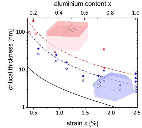
Figure 1: Critical thickness for plastic relaxation of c-plane strained wurtzite films. Dashed and solid lines correspond to calculated critical thicknesses according to the new results depending on the surface morphology and the old model. Symbols represent experimental data.
Whether relaxing the strain between two layers caused by the lattice mismatch or growing pseudomorphic defect-free heterojunctions, it is critical to understand under which conditions and how misfit dislocations form in the material. Previous quantitative studies of plastic relaxation in wurtzite films adopted the classical models deduced from cubic materials (InGaAs on GaAs, SiGe on Si). In these works, the authors only considered the energy balance aspect, i.e. the moment when plastic relaxation becomes energetically favourable, while completely neglecting the nucleation process of misfit dislocations itself. However, for wurtzite materials, it is particularly important to consider this process, due to the limitation of how dislocations can move within the wurtzite crystal lattice. As an outcome, a significant discrepancy between theoretical predictions and experimental observations of plastic relaxation in III-nitride thin films has existed for many years.
The current study combines thorough experimental analysis of dislocation formation in AlGaN/GaN heterostructures at each growth step by using transmission electron microscopy (TEM), scanning electron microscopy (SEM) and atomic force microscopy (AFM) techniques, together with theoretical calculations of the stress distribution at the dislocation nucleation sites obtained from the finite-element method.
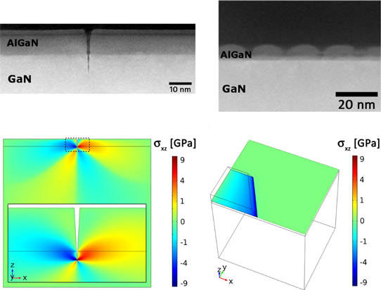
Figure 2: Top: cross-sectional scanning TEM images of AlGaN/GaN heterostructures - two-dimensional layer with a crack (left) and three-dimensional islands (right). Bottom: shear stress calculated for the same surface structures as observed in the experiment.
“We have found that, for c-plane wurtzite films, only the presence of three-dimensional surface structures – islands’ edges and corners, crack fronts, surface macro-steps or V-pits – and the high concentration of the shear stress at these sites enables the nucleation and spread of misfit dislocations in the interfacial plane,” says author Dr Toni Markurt of the Leibniz Institute for Crystal Growth. “This provides an efficient pathway for the plastic relaxation.”
More importantly, according to the authors, the critical thickness of the films strongly depends on the surface morphology and the actual geometry of surface structures: for example, two-dimensional layers with cracks can be grown thicker than films with three-dimensional islands, before undergoing plastic relaxation.
The work was performed in close collaboration with Osram Opto Semiconductors GmbH of Regensburg, Germany, which provided dedicated samples for the experimental study.
https://aip.scitation.org/doi/10.1063/1.5025813


