


- News
30 July 2018
Structures to enhance light extraction in indium gallium nitride LEDs
Yu-Lin Lee and Wen-Chau Liu of Taiwan’s National Cheng Kung University have been working to enhance light extraction from indium gallium nitride (InGaN) light-emitting diodes (LEDs) by using texturing of the mesa top surface and sidewalls [IEEE Transactions on Electron Devices, published online 4 July 2018]. In particular, the researchers created a micro-hole array on the top surface and either 45° saw-tooth or convex patterning of the sidewalls.
The aim of these measures is to increase the probability that photons will escape from the structure into the outside world. InGaN-based devices are prone to reflect light back into the device at GaN/air interfaces. Total internal reflection occurs due to the large difference in refractive index between GaN and air, giving a relatively narrow escape cone for photons. The texturing is designed to reduce total internal reflection, boosting light extraction efficiency.
One such structure demonstrated increases of 20.9%, 24.3%, 20.5% and 21.3% in light output power, luminous flux, external quantum efficiency and wall-plug efficiency, respectively, over a reference device without micro-hole array or sidewall texturing.
Metal-organic chemical vapor deposition (MOCVD) on c-plane sapphire produced an LED wafer with a 2μm undoped GaN buffer, 2μm silicon-doped n-GaN contact, 15-period InGaN/GaN active multiple quantum wells (MQWs), and a 0.3μm magnesium-doped p-GaN contact.
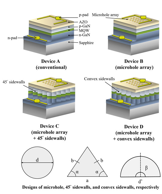
Figure 1: Schematic cross-sectional diagrams and corresponding geometric designs of devices A-D.
Fabricated devices (Figure 1) had varying mesa sidewall structures: flat (A and B), 45° saw-tooth (C), and convex (D). Also, devices B-D included a micro-hole array on the top surface. The mesa and micro-hole etching included inductively coupled plasma (ICP) and wet processes. The circular micro-holes were 7μm in diameter. The saw-tooth sidewalls of device C consisted of 45° (angle α) isosceles triangles with a 10μm hypoteneuse (side a). The diameter of the convex sidewall of device D sections was 10μm.
The fabrication process flow included cleaning, ICP definition of the LED mesa, sidewalls and micro-hole array, sputtering of a 500nm aluminum-doped zinc oxide (AZO) current-spreading layer (CSL), wet etching of the AZO current-spreading layer to expose the micro-hole array, annealing of the AZO current-spreading layer, and the deposition of chromium/platinum/gold n- and p-pads.
After processing, the micro-holes had 7μm diameter at the GaN surface and 16μm diameter at the AZO surface. The use of the AZO current-spreading layer avoided problems associated with indium tin oxide (ITO) as transparent conductor in terms of cost, toxicity and thermal stability, among other properties. The 650μmx550μm LED chips were attached and bonded onto TO-3 submounts for testing.
All the devices had a forward voltage of 2.95V for 20mA injection. This increased to 4.35V for 200mA. The leakage at -5V reverse bias was 13.3nA.
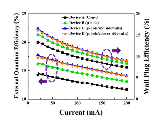
Figure 2: External quantum efficiency and wall-plug efficiency as functions of operating current.
The light output power at 200mA injection ranged from 65mW for device A, through 72.8mW (B) and 78.2mW (D), reaching 78.6mW for device C. These improvements are also reflected in terms of luminous flux, luminous efficacy, external quantum efficiency and wall-plug efficiency (Figure 2 and Table 1). In all cases, the devices C and D show significant improvement over the reference A, with device C having a slight edge over D.
Table 1: Performance characteristics at 200mA injection.
| Characteristic | A | B | C | D |
| Light output power | 65mW | 72.8mW | 78.6mW | 78.2mW |
| Luminous flux | 2.18lm | 2.55lm | 2.71lm | 2.69lm |
| Luminous efficacy | 2.5lm/W | 2.9lm/W | 3.1lm/W | 3.0lm/W |
| External quantum efficiency | 11.7% | 13.1% | 14.1% | 14% |
| Wall-plug efficiency | 7.5% | 8.4% | 9.1% | 8.9% |
The increased light emission from the enhanced sidewall structures was reflected in increased far-field divergent angles over that of device A (132°): 139° for B, 141° for C, and 141° for D.
https://doi.org/10.1109/TED.2018.2849353
The author Mike Cooke is a freelance technology journalist who has worked in the semiconductor and advanced technology sectors since 1997.


