


- News
4 July 2018
Tokyo Institute of Technology develops n- and p-type copper nitride semiconductor for environmentally friendly thin-film photovoltaics
© Semiconductor Today Magazine / Juno PublishiPicture: Disco’s DAL7440 KABRA laser saw.
By using a unique nitriding technique applicable for mass production and a computational search for appropriate doping elements (as well as atomically resolved microscopy and electronic structure analysis using synchrotron radiation), Tokyo Institute of Technology has shown that copper nitride (Cu3N) acts as an n-type semiconductor, with p-type conduction provided by fluorine doping (Kosuke Matsuzaki et al, ‘High‐Mobility p‐Type and n‐Type Copper Nitride Semiconductors by Direct Nitriding Synthesis and In Silico Doping Design’). These n-type and p-type copper nitride semiconductors could potentially replace the conventional toxic or rare materials in photovoltaic cells, it is reckoned.
Compared to market-dominating silicon solar panels, thin-film photovoltaics have equivalent efficiency and can cut the cost of materials. The technology allows low-cost and scalable manufacturing routes compared to crystalline silicon technology, even though toxic and rare materials are used in commercialized thin-film solar cells. Tokyo Institute of Technology aims to find a new candidate material for producing cleaner, cheaper thin-film photovoltaics.
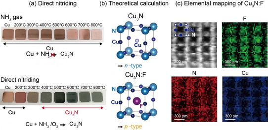
(a) Thin-film copper plates before and after reacting with ammonia and oxygen. Copper metal has been transformed to copper nitride. (b) Copper insertion for n-type semiconductor and fluorine insertion for p-type semiconductor. (c) Nitrogen plotted in red, fluorine in green, and copper in blue. Fluorine is located at the open space of the crystal, as predicted by theoretical calculation.
The team has focused on a simple binary compound, copper nitride, composed of environmentally friendly elements. However, growing a nitride crystal in a high-quality form is challenging, as history shows from the development of gallium nitride (GaN) blue LEDs. Matsuzaki and his coworkers have overcome the difficulty by introducing a novel catalytic reaction route (gaseous direct nitriding) using ammonia and oxidant gas, applicable to uniform and large‐area deposition. This compound – see the photograph in figure (a) – is an n-type conductor with excess electrons. On the other hand, by inserting the element fluorine in the open space of the crystal, this n-type compound was transformed into p-type, as predicted by density functional theory calculations and directly proven by atomically resolved microscopy in figures (b) and (c), respectively.
All existing thin-film photovoltaics require a p-type or n-type partner in their makeup of a sandwich structure, requiring great effort to find the best combination. The p-type and n-type conduction in the same material developed by Matsuzaki and his coworkers are beneficial for designing a highly efficient solar cell structure without such efforts. The material is also non-toxic, abundant and hence potentially cheap – a suitable replacement for cadmium telluride (CdTe) and copper indium gallium diselenide (CIGS) thin-film solar cells. Tokyo Institute of Technology reckons that, with the development of these p-type and n-type semiconductors in a scalable forming technique using simple, safe and abundant elements, the positive qualities will help to bring thin-film photovoltaics to greater prominence.
Tokyo Institute of Technology Thin-film PV
http://dx.doi.org/10.1002/adma.201801968


