


- News
25 June 2018
3D-Micromac launches selective laser annealing system
© Semiconductor Today Magazine / Juno PublishiPicture: Disco’s DAL7440 KABRA laser saw.
3D-Micromac AG of Chemnitz, Germany (which provides laser micromachining and roll-to-roll laser systems for the semiconductor, photovoltaic, medical device and electronics markets) has unveiled the microPRO RTP, its new laser annealing system designed to enable several key process steps in semiconductor, power device and MEMS manufacturing. Combining a laser optic module with 3D-Micromac’s modular semiconductor wafer processing platform, the microPRO RTP provides selective annealing with high repeatability and throughput in a versatile system.
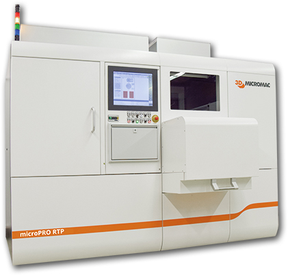
Picture: 3D-Micromac’s microPRO RTP system.
The microPRO RTP features a line-scan option for vertical selective annealing and a step-and-repeat spot option for horizontal selective annealing, as well as three optional laser wavelengths (near-infrared, green and ultraviolet). It addresses applications including:
- Dopant activation for insulated-gate bipolar transistors (IGBTs), as well as activation of backside-illuminated (BSI) CMOS image sensors and amorphous silicon (a-Si) - the microPRO RTP uses a high-speed line scan with what is claimed to be excellent energy homogeneity and repeatability to provide precise localization of the field stop layer, which minimizes heat transference to the front-side of the wafer.
- Ohmic contact formation in silicon carbide (SiC) power devices to improve resistance - using spot scanning with short laser pulses, microPRO RTP can process the entire metalized backside of SiC wafers, forming ohmic interfaces and curing grinding defects, while preventing the generation of large carbon clusters and heat-related damage to the front-side of the wafer.
- Giant magneto resistive (GMR) and tunneling magneto resistive (TMR) sensor manufacturing - using a selective step-and-repeat spot and variable laser energy, microPRO RTP can selectively heat functional areas on the sensor to form and orient the magnetic fields for these MEMS sensor types.
“As microelectronics adopt 3D/stacked architectures to achieve more functionality, manufacturers need annealing solutions that can process the surface layers of their devices without affecting buried structures underneath,” says product manager Hans-Ulrich Zühlke. “The migration to new materials and heterogeneous integration adds even more complexity to the annealing process, driving the need for selective exposure of functional areas, which only selective laser annealing can provide,” he adds. “Leveraging our years of experience in providing laser solutions to the semiconductor and microelectronics market, 3D-Micromac is pleased to offer our new microPRO RTP laser annealing solution, which provides the selectivity, flexibility and throughput our customers need to meet their unique annealing requirements.”
Advantages that the microPRO RTP is said to provide compared with existing annealing methods include:
- high precision and repeatability in both X and Y directions;
- high selectivity to different substrates and films, with multiple options for laser pulse length, energy and overlap to ensure no damage to the area surrounding the target site;
- very high energy homogeneity’
- precise process monitoring; and
- flexibility to handle substrate diameters ranging from 50mm up to 300mm.
3D-Micromac is exhibiting in booth #1645 (South Hall) at SEMICON West 2018 at the Moscone Convention Center in San Francisco, CA, USA (10-12 July).


