


- News
8 June 2018
Expanding the application potential of hydride vapor phase epitaxy
SCIOCS Co Ltd in Japan has been developing its hydride vapor phase epitaxy (HVPE) technology and has recently reported with Japan’s Hosei University its use as an alternative to metal-organic chemical vapor deposition (MOCVD) as a means to create very lightly doped n-type gallium nitride (GaN) drift layers for vertical power devices. SCIOCS’ researchers believe that device-quality smooth as-grown surfaces with good thickness uniformity can be achieved using HVPE that are comparable with the results of MOCVD. Traditionally, HVPE has been seen as a means to growing thick layers relatively quickly, but with a lower structural quality.
In addition, the company’s researchers have used HVPE to create 6mm-thick free-standing GaN crystals with diameters up to 6 inches.
Vertical diode
Drift layers in vertical power devices extend the distance over which a potential drops, reducing the electric field and hence increasing breakdown voltages. Epitaxial material for the vertical diode developed with Hosei University was grown on 2-inch free-standing silicon-doped n-GaN substrates [Hajime Fujikura et al, Appl. Phys. Express, vol11, p045502, 2018]. The free-standing substrates were prepared using a void-assisted separation method developed by the researchers in the period 2003-2017 (see below). The threading dislocation density was uniform in the range (1-3)x106/cm2.
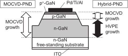
Figure 1: Schematic structure of PN-junction diode.
The new structure with epitaxial growth combined HVPE and MOCVD methods (Figure 1) was compared with an MOCVD-only process. The MOCVD-only method required a rather complex n-type drift layer structure (Figure 2). The MOCVD regrowth on HVPE material was prepared with a hydrofluoric cleaning process.
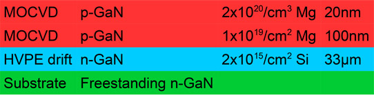
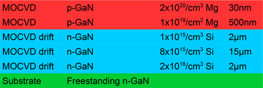
Figure 2: (a) HVPE/MOCVD epitaxial structure. (b) MOCVD-only structure.
The fabrication of the vertical pn diode (PND) involved mesa etching for isolation and deposition of diode electrodes consisting of palladium/titanium/gold (Pd/Ti/Au) and indium tin oxide (ITO) for the p- and n-contacts, respectively.
The researchers used an HVPE chamber without quartz parts, as developed by SCIOCS last year [see e.g. Hajime Fujikura et al, Jpn. J. Appl. Phys., vol56, p085503, 2017]. Quartz consists of silicon dioxide. Silicon and oxygen are donor impurities in GaN. The use of HVPE also avoids carbon incorporation, which is a problem with the metal-organic precursors of MOCVD.
In a quartz-based HVPE system unintended silicon impurity concentration can be of the order 1x10¹⁷/cm3, while oxygen incorporation is of the order 8x10¹⁵/cm3. Removing quartz parts can give a silicon level of less than 1x10¹⁶/cm3. In their 2017 research, the SCIOCS team found that the oxygen content was below the detection limit of its secondary-ion mass spectroscopy (SIMS) system. Further optimization enabled the researchers to reduce the silicon concentration to below the SIMS detection limit too (5x10¹⁴/cm3). “To the best of our knowledge, this is the purest GaN layer ever reported to date,” the researchers commented at the time.
The layer was also highly resistive (more than 1x10⁹Ω-cm). Such high resistivity could be the base for devices built using ion-implantation of silicon and magnesium impurity doping, as in mainstream silicon electronics. The mobility of n-GaN layers with 1x10¹⁵/cm3 electron concentration was 1150cm2/V-s.
For the more recent research on vertical diodes, the use of quartz-free HVPE was found to reduce non-uniform conductivity due to carbon incorporation and uncontrolled silicon impurity concentration in the drift layer. Non-uniformity was detected by studying electroluminescence variations under a microscope.
Carbon incorporation and the resulting compensation effects in MOCVD material is non-uniform due to the presence of macrosteps of the scale of several tens of microns on the growth surface. The absence of carbon in the HVPE drift layer was confirmed by secondary-ion mass spectrometry (SIMS).
The team comments: “The absence of carbon compensation and in-plane carrier concentration modulation will make it easy to grow power device structures as they are designed, and hence enable the design of devices with performance reaching the material limitations. Additionally, the absence of off-angle-dependent carrier concentration changes will improve the uniformity and reproducibility of device performance, leading to improved yield in mass production of GaN-based power devices, even if off-angle differences exist within given wafers and/or between wafers.”
Off-angle variations arise due to wafer bowing.
A hybrid MOCVD/HVPE diode with 200μm diameter achieved a high breakdown of ~2kV and relatively low on-resistance of 2mΩ-cm2 (Figure 3). The device did not have a field plate structure to avoid field concentration effects at electrode edges. There was some leakage at low forward bias and the ideality was around 2 rather than the ~1-ideality achieved in the comparison MOCVD-only structure.
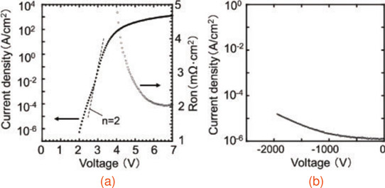
Figure 3: (a) Forward and (b) reverse I–V characteristics of hybrid pn diode made by MOCVD re-growth on HVPE-grown GaN drift layer.
The researchers comment: “This deterioration could be attributed to dominance of the recombination current through defect and/or impurity levels within the bandgap due to the presence of accumulated silicon at the re-grown interface. However, all of these observed characteristics of the present hybrid pn diode were superior to those recently reported for a similar pn diode having an MOCVD-grown drift layer and a p-GaN layer re-grown by molecular beam epitaxy.”
Substrate
SCOICS researchers also used their void-assisted separation method to create 6mm-thick GaN crystals with diameters up to 4 inches [Hajime Fujikura et al, Jpn. J. Appl. Phys., vol57, p065502, 2018]. The team reports that a 6-inch wafer is being process, but has not yet been characterized: “However, with the availability of similar thick 6-inch bulk crystals as for the 2- and 4-inch crystals, we expect the fabrication of high-quality, macro-defect-free 6-inch GaN wafers from this bulk crystal in the near future.”
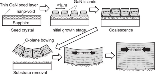
Figure 4: Sequence of void-assisted separation method.
Void-assisted separation consists mainly of HVPE growth on sapphire (Figure 4). First MOCVD is used to create a thin GaN seed layer with many nanometer-size voids. The HVPE GaN first forms islands on the MOVPE material, which then coalesce and bow the wafer. As the growth proceeds, the bowing becomes less extreme.
The material tends to be less prone to macro-defects, compared with epitaxial layer overgrowth methods, since the GaN from the small islands of the seed layer more quickly coalesces. Macro-defects include pits, high-threading dislocation density (TDD) regions, inversion domains (IDs), through-holes, and cracks.
As the bowing reduces, there are a number of sources of the stress that can lead to cracking. Some stress arises from the bowing reduction. Stress also arises at the edge of the wafer due to increased impurity incorporation compared with the bulk. The edge stress can be reduced by slicing and polishing the final freestanding GaN substrate.
The HVPE process used GaCl as the metal-hydride source. The GaCl was created by flowing hydrochloric (HCl) gas over gallium at 800°C. The nitrogen component of GaN came from ammonia (NH3). The HVPE growth temperature was typically 1050°C. The resulting GaN substrates ranged in thickness from 100μm (0.1mm) to more than 6mm.
The researchers found that the presence of macro-defects allowed the growth of thick GaN substrates without stress-induced cracking or breakage. Macro-defects reduce internal stress since crystal imperfection gives additional freedom for crystal deformation. However, macro-defects make it difficult to produce practical devices with high yield.
The team has therefore studied ways to use increase hardness to overcome the tradeoff by increasing the critical stress allowed in the GaN crystal. The hardness increase was achieved by controlling the HVPE growth conditions to reduce potential for plastic deformation. In previous work, the hardness of GaN substrates was increased from 19.7GPa to 20.1GPa and even 20.7GPa (samples A-C, respectively). The higher hardness value allowed the team to reduce threading dislocation densities (TDDs) even below 1x10⁶/cm2, compared with 5x10⁶/cm2 for the 19.7GPa initial sample. The 20.7GPa hardness process enabled GaN thicknesses up to 2mm without cracking.
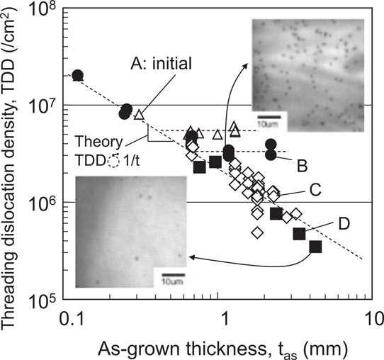
Figure 5: Relationships between as-grown thickness (tas) and TDD for macro-defect-free GaN substrates grown by void-assisted separation method using conditions A–D. Insets: cathodoluminescence (CL) images for GaN substrates grown using conditions B and D.
Building on this work, the researchers achieved 22GPa hardness, allowing GaN thickness to reach 6mm without macro-defects in a 55mm-diameter substrate (2.17 inches). The sample (D) also showed much reduced TDD to the mid-105/cm2 range (Figure 5). Sample D did not show any tendency for the reduction of TDD with as-grown thickness to saturate. The new growth process for sample D also eliminated basal plane dislocations, allowing for increased thickness. The off-angle variation was less than 0.1°.
The researchers used their technology to realize 4-inch and 6-inch free-standing macro-defect-free GaN wafers with thicknesses of more than 3mm. Off angle variation was 0.2° for the 4-inch substrate, and the TDD was in the 105/cm2 range.
https://doi.org/10.7567/APEX.11.045502
https://doi.org/10.7567/JJAP.57.065502
https://doi.org/10.7567/JJAP.56.085503
https://www.sciocs.com/english/
The author Mike Cooke is a freelance technology journalist who has worked in the semiconductor and advanced technology sectors since 1997.


