


- News
7 March 2018
Vanadium dioxide enables III-nitride phase-transition field-effect transistor
Cornell University and US Naval Research Laboratory in the USA has demonstrated a gallium nitride (GaN) phase-transition field-effect transistor (FET) based on loading a metal-oxide-semiconductor high-electron-mobility transistor (MOS-HEMT) with a vanadium dioxide (VO2) resistor [Amit Verma et al, IEEE Transactions on Electron Devices, vol65, p945, 2018]. The combination enabled very low leakage along with ‘sub-thermionic’ subthreshold steep-switching behavior.
The researchers comment: “This first demonstration of ultralow-leakage steep switching in GaN phase-FETs using integration-friendly ALD VO2 opens the door to introducing new functionalities in nitride low-power digital devices, microwave circuits, photonic devices, and power electronics in the GaN-on-silicon platform.”
Heating the VO2 resistor above ~67°C gave an insulator to metal transition. An electrically driven transition to the metallic phase occurred above a critical field of ~27kV/cm at 60°C. The current density threshold was ~20μA/μm.
The VO2 was grown by atomic layer deposition (ALD) using tetrakis-ethylmethylamino-vanadium (TEMAV) and ozone precursors on sapphire. The layer was 50nm thick with amorphous structure. Annealing crystallized the VO2. The contacts on the 100μm-wide VO2 resistors were titanium/gold.
The team comments: “Though this transition can be achieved at room temperature, an elevated temperature of 60°C was used to keep the transition voltage lower.”
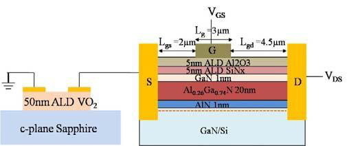
Figure 1: Schematic of phase-FET. AlGaN/GaN MOS-HEMT on Si (right) loaded at source with ALD VO2 resistor.
The resistor was connected to an aluminium gallium nitride barrier (AlGaN) MOS-HEMT on silicon (Figure 1). The GaN buffer layer was 1.3μm. The ohmic source/drain contacts were alloyed titanium/aluminium/nickel/gold. The gate stack consisted of ALD silicon nitride (SiNx) and alumium oxide (Al2O3) with nickel/gold electrode.
Without the VO2 load resistor, the pinch-off voltage was -5V, while the on/off current ratio was 12 orders of magnitude. At 60°C, the subthreshold swing/slope (SS) was ~90mV/decade, which compares with the thermionic ‘Boltzmann’ limit of 66mV/decade. Good saturation gave current densities of ~0.4mA/μm.
The phase FET consisted of a 2μmx100μm VO2 source load on a 200μm-wide GaN MOS-HEMT with 3μm gate length, and 2μm gate-source and 4.5μm gate-drain separations. The performance of the combined device depended on the direction of sweep (hysteresis).
In the insulating state, the VO2 load reduces the effective gate-source bias, suppressing the drain current. There is also an impact when the VO2 resistor goes metallic: with the drain bias at 10V and the gate at +2V, the drain current was 337μA/μm, while in the bare MOS-HEMT the current was 427μA/μm under the same conditions. Due to the extremely low off-current, the VO2 resistor has “no effect” in the off-state.
The transition from insulating to metallic phase for the VO2 resistor occurred at a drain bias of about 4V in up-sweeps. The change back to insulating VO2 was more gradual in the down sweep.
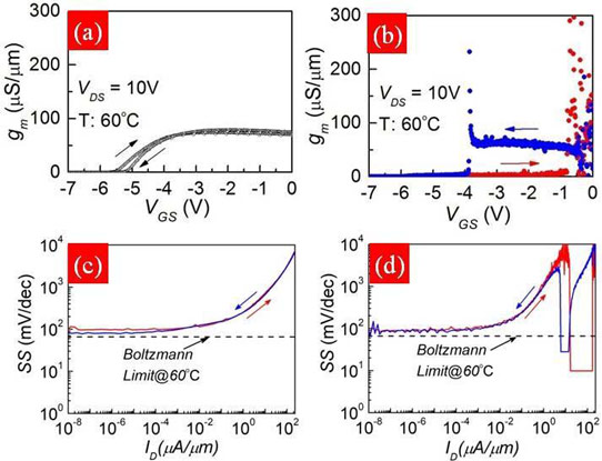
Figure 2: Measured transconductance of (a) GaN MOS-HEMT and (b) GaN phase-FET as function of gate bias. Measured SS as function of drain current for (c) GaN MOS-HEMT and (d) GaN phase-FET device at 60°C.
The SS behavior showed the MOS-HEMT being above the thermionic limit at all times (Figure 2). However, the phase FET had values reaching down to ~9mV/decade in the up-sweep and ~29.2mV/decade in the down-sweep. At the same drain currents as these minima, the MOS-HEMT SS was ~720mV/decade.
The researchers comment: “This experimental result is an initial proof of concept to access sub-Boltzmann limit modulation using ALD VO2. To move the steep transition gate voltages to the subthreshold regime for low-power digital switching, and potentially for memory-logic hybrids, it will be necessary to match the device geometries and the VO2 impedance. This will also enable shaping of the hysteresis.”
The team sees the next steps of the research as being on-wafer integration of the two components of the phase-FET, reducing hysteresis, reducing the VO2 phase transition voltage at room temperature, and obtaining steep switching over a larger drain current range.
GaN Fet MOS-HEMT Vanadium dioxide resistor ALD
https://doi.org/10.1109/TED.2018.2795105
The author Mike Cooke is a freelance technology journalist who has worked in the semiconductor and advanced technology sectors since 1997.


