


- News
20 March 2018
Indium arsenide channel transistors for mm-wave and high-speed applications
University of California Santa Barbara (UCSB) in the USA claims a record 420GHz maximum oscillation frequency (fmax) for a III-V metal-oxide-semiconductor field-effect transistor (MOSFET) based on indium gallium arsenide (InGaAs) layers on semi-insulating iron-doped (100) indium phosphide (InP:Fe) substrate [Jun Wu et al, IEEE Electron Device Letters, published online 8 February 2018]. The conduction channel was InAs.
The design reduced parasitic gate-source and gate-drain capacitances through increasing the lateral modulation-doped access region, giving a wider separation of the gate and source-drain regions. The researchers see the devices as promising candidates for high-speed applications, particularly millimeter (mm)-wave.
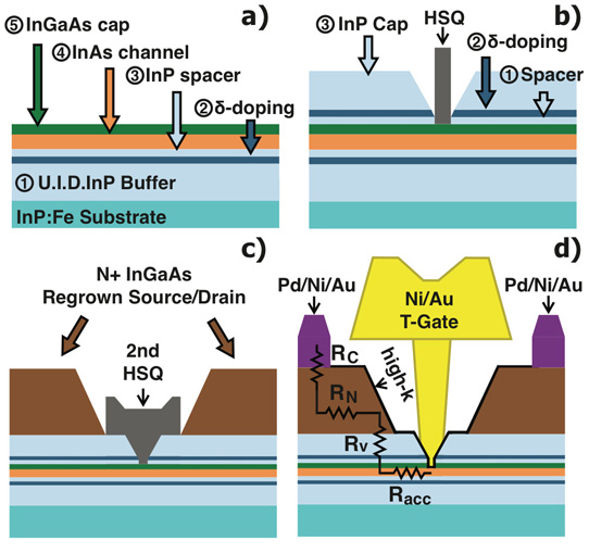
Figure 1: (a-c) Schematic of MOSFET processing. (d) Final device with definitions of contact resistance (RC), regrown N+ contact film resistance (RN), vertical resistance through InP layer (RV), and access resistance (Racc).
Metal-organic vapor phase epitaxy deposited a 10nm unintentionally doped (U.I.D.) InP buffer, 2nm silicon-doped InP (δ-doping), 2nm U.I,D InP spacer, 5nm strained InAs channel, and a 3nm U.I.D. In0.53Ga0.47As cap (Figure 1). A low growth temperature of 500°C was used for the channel layer, along with a low 7.8 V/III ratio.
A dummy gate of hydrogen silesequioxane (HSQ) was fabricated before further MOVPE growth of a 2nm U.I.D. InP spacer, 2nm silicon-doped InP, and 10nm U.I.D. InP cap. The dummy gate was removed and replaced by a wider dummy gate, creating 50nm access regions for regrown source-drain layers of 80nm-thick highly doped (N+) InGaAs.
The transistor fabrication consisted of mesa isolation, dummy gate removal, digital etch of the InGaAs cap from the channel, nitrogen-plasma and tri-methyl-aluminium passivation and atomic layer deposition of 3nm zirconium dioxide high-k dielectric, deposition of palladium/nickel/gold (Pd/Ni/Au) source-drain contacts, and Ni/Au T-gate formation.
A device with 30nm gate length had 1.5mS/μm peak extrinsic transconductance with 0.5V drain bias. The peak came at 0.3V gate potential. The minimum sub-threshold swing was 90mV/decade. The off-state (-0.1V gate) current was 0.9μA/μm.
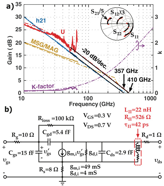
Figure 2: (a) Measured (solid curves) and modeled (dashed curves) current gain, unilateral power gain, maximum stable/available gain and stability factors at 0.3V gate and 0.7V drain. Solid black lines indicate -20dB/decade extrapolations from 30-50GHz region to determine ft and fmax. Inset: measured (red) and modeled (black) S-parameters. (b) Small-signal equivalent circuit model.
Frequency performance was measured between 10MHz and 67GHz on a device with two 10μm gate fingers (Figure 2). De-embedding gave an extrapolated cut-off frequency (ft) of 357GHz and fmax of 410GHz with 0.7V drain and 0.3V gate bias. Reducing the gate voltage to 0.2V increased fmax to 420GHz, but at the cost of reducing ft.
A shorter 16nm gate length resulted in reduced fmax, but similar ft. The degraded fmax was blamed on short-channel effects giving an increased output conductance (gd,i).
MOSFET InGaAs InP:Fe substrate MOVPE
https://doi.org/10.1109/LED.2018.2803786
The author Mike Cooke is a freelance technology journalist who has worked in the semiconductor and advanced technology sectors since 1997.


