


- News
16 May 2018
High-voltage gallium oxide transistors with more than 1kV breakdown
Researchers based in the USA and Japan claim the first enhancement-mode high-voltage vertical gallium oxide (Ga2O3) metal-insulator-semiconductor field-effect transistors (MISFETs) [Zongyang Hu et al, IEEE Electron Device Letters, published online 25 April 2018]. Enhancement-mode operation (normally-off at 0V gate) is highly desired for power electronics, reducing power consumption and allowing for fail-safe designs.
Ga2O3 has a wide 4.9eV bandgap and expected 8MV/cm breakdown field. The electron mobility has a decent limit of 250cm2/V-s, allowing realistic power device proposals. Large single-crystal substrates are commercially available.
Cornell University in the USA and Hosei University and Novel Crystal Technology Inc in Japan used hydride vapor phase epitaxy (HVPE) to deposit 10μm n-Ga2O3 on n-Ga2O3 (001) substrate. The substrate carrier density was 2x10¹⁸/cm3. The epitaxial drift layer doping concentration was less than 2x10¹⁶/cm3. A silicon box-implant added a 50nm n+-Ga2O3 layer with 5x10¹⁹/cm2 doping to allow low contact resistance for the source contact after activation annealing.
Vertical fin-channels were inductively coupled etched using platinum masking. The target fin height and width were 1.0μm and 0.3μm, respectively. The gate stack consisted of atomic layer deposition (ALD) aluminium oxide (Al2O3) dielectric and sputtered chromium (Cr) metal.
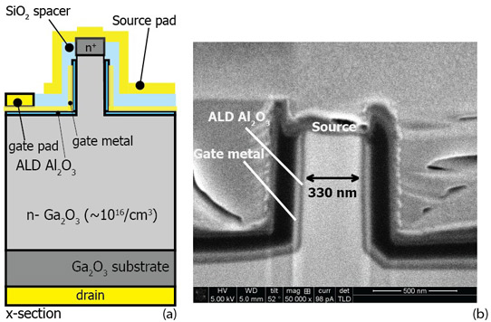
Figure 1: (a) Schematic cross section of Ga2O3 vertical power MISFET. (b) 52° scanning electron microscope SEM cross-section image showing 330nm wide and 795nm long fin-channel.
Photoresist fill and planarization steps were used to remove metal from the 50nm n+-Ga2O3 source contact material. Plasma-enhanced chemical vapor deposition (PECVD) of 200nm silicon dioxide (SiO2) spacer was followed by resist fill and planariazation to clear the source contact region again. The ohmic source titanium/aluminium/platinum (Ti/Al/Pt) metals were then deposited. Devices (Figure 1) were isolated by removing SiO2 and Cr from between them.
Devices with 0.33μmx80μm source area had a drain current density of ~350A/cm2 with 10V drain bias and the gate set at 3V under pulsed operation, avoiding thermal effects. The differential on-resistance was ~18mΩ-cm2, normalized to the source contact area. Process non-uniformity led to a wide range of drain currents (300-500A/cm2) and on-resistances (13-18mΩ-cm2). Threshold voltages were all positive, in the range +1.2V-+2.2V, giving enhancement-mode, normally-off operation. The on/off current ratio was of the order 108. The leakage was at the limit of the measurement system. The sub-threshold swing was ~85mV/decade.
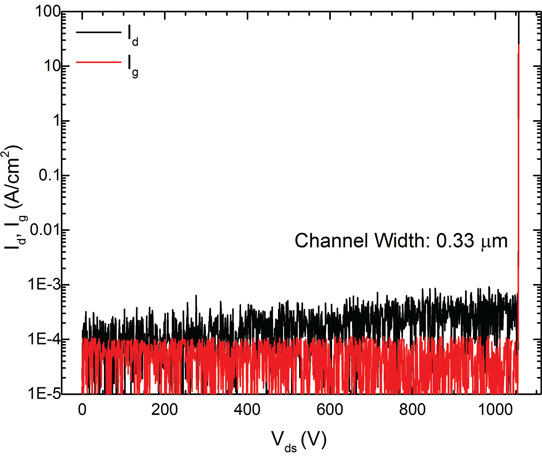
Figure 2: Representative three-terminal off-state (at 0V gate) drain and gate current versus drain bias (Id/Ig -Vds) characteristics and breakdown voltage.
Hard breakdown occurred at 1057V drain voltage (BV) with leakage current low at close to the detection limit up to that point (Figure 2). The breakdown field is estimated at 1.44MV/cm, far below the value expected for Ga2O3.
The researchers comment: “Examination of the devices after breakdown shows visible damage near the outer edges of the gate pads. For the same reason, the three-terminal BV demonstrated in this work is slightly lower compared to the two-terminal BVs in heterojunction p-Cu2O/n-Ga2O3 diode fabricated on similar HVPE-Ga2O3 epitaxial layers and substrates.” The team expects higher breakdown voltages from implementing field plates or ion implantation edge termination.
https://doi.org/10.1109/LED.2018.2830184
The author Mike Cooke is a freelance technology journalist who has worked in the semiconductor and advanced technology sectors since 1997.


