


- News
11 May 2018
Normally-off gallium nitride nanowire transistors with inverted p-channel
Researchers based in Germany claim the first vertical gallium nitride (GaN) nanowire (NW) metal-oxide-semiconductor field-effect transistors (MOSFETs) with an inverted channel, allowing a positive 2.5V threshold voltage and giving enhancement-mode normally-off behavior [Feng Yu et al, IEEE Transactions On Electron Devices, published online 19 April 2018].
The high threshold was achieved by using p-GaN as the channel material. With 0V on the gate, the channel blocks current flow. Increasing the gate potential inverts the channel, increasing the electron density and allowing transport.
The team from Technische Universität Braunschweig, Universität Kassel and Physikalisch-Technische Bundesanstalt sees advantages from GaN electronics over silicon as including “switching speed, operation temperature, output power, as well as radiation immunity”. Logic and switching applications prefer circuit designs based on normally-off enhancement-mode transistors.
Metal-organic vapor phase epitaxy created a GaN structure with different doping levels on c-plane sapphire (Figure 1). The vertical nanowires were created through patterning with a chromium (Cr) mask and etching with sulfur hexafluoride inductively coupled plasma.
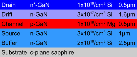
Figure 1: Epitaxial structure.
The nanowires were ~1μm diameter and 2.8μm high. The pitch between the wires was 4μm. Further wet etching with AZ400K developer was performed to smooth the wire surfaces and remove other damage from the dry etch.
In fact, the wires had non-uniform diameter of 1.3μm at the bottom and 0.85μm at the top after dry etching. The wet etch also resulted in vertical wires of 0.47μm diameter and ‘mushroom’ top just under the Cr mask.
The magnesium (Mg) doping of the buried p-GaN layer was activated with rapid thermal annealing (RTA) – 30 seconds at 950°C and 5 minutes at 600°C. The larger surface area of the nanowire structure allowed passivating species such as hydrogen to escape. In normal epitaxial structures, the p-GaN layers are deposited last, since buried p-GaN layers are not able to expel passivating atoms.
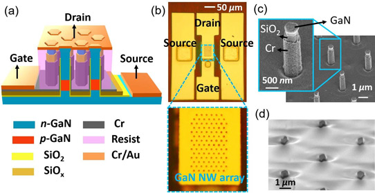
Figure 2: (a) Schematic and (b) microphotograph of fabricated vertical GaN nanowire-based MOSFET with inverted p-GaN channel. 45°-tilted scanning electron microscope images (c) before and (d) after filling with resist.
The MOSFET (Figure 2) was produced with 25nm plasma-enhanced atomic layer deposition silicon dioxide (SiO2) on the wire sidewalls, and 200nm silicon oxide (SiOx). The gate metal was 300nm electron-beam-evaporated chromium. The space between the wires was filled with photoresist. The resist was etched back and refilled a number of times to enable selective removals of chromium and silicon oxide. The resist was finally cured and chromium/gold electrodes formed.
The MOSFET consisted of 103 nanowires. The gate length of 0.5μm was defined by the thickness of the p-GaN layer. The width was given by the combined circumferences of the nanowires. The device area was 1.4x10⁻⁵cm2. The ohmic source-drain contacts were not ideal.
The maximum drive current (Id) at 6V gate potential was 18mA. The current density in the wires was 101kA/cm2. The specific on-resistance was small at 5.3mΩ-cm2, including the space between the wires. The threshold voltage (Vth) was +2.5V and the normalized peak transconductance was 41mS/mm. The on/off current ratio was of the order of 109. The subthreshold swing was 120mV/decade, rather high compared with previous devices. The large swing was tentatively attributed to a high trap density at the p-GaN/SiO2 interface in the gate region. Breakdown with 0V gate came at 69V drain bias.
Some gate-bias-dependent hysteresis was found which the researchers suggest was due to “positive charging close to or at the channel region, especially at high gate bias”. They comment: “The hysteresis brings instability in both Vth and Id, which would limit the device application in high-frequency switching.”
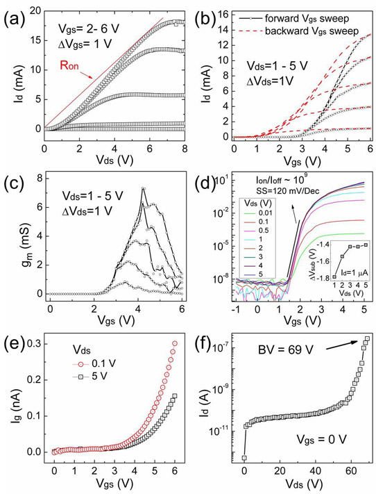
Figure 3: Electrical characteristics of vertical GaN MOSFET consisting of 103 nanowires. (a) Output characteristic. (b) Transfer characteristic under bidirectional gate sweep with rate of 0.8V/s. (c) Transconductance (gm) characteristic of forward gate transfer in (b). (d) Subthreshold characteristic under the forward-gate sweep. Inset: corresponding voltage shift (ΔVsub) at Id of 1μA during bidirectional gate sweep. (e) Gate leakage at drain bias Vds of 0.1V and 5V. (f) Breakdown voltage (BV) test at 0V gate potential (Vgs).
The team considers mobile ions as the most likely cause of the hysteresis. They comment: “The mobile ions in SiO2 could be primarily alkaline impurities introduced unintentionally during the device processing, e.g. alkaline involved wet etching and photoresist curing”. The researchers suggest that aluminium oxide or silicon nitride would be preferable dielectrics, compared with silicon dioxide, allowing alkaline-free processing.
The researchers compared their inverted p-GaN channel device with n-GaN channel NW MOSFETs – the p-GaN allowed a higher threshold than the competitors, some of which had negative values, indicating depletion-mode normally-on behavior. The p-GaN device also demonstrated high values for the normalized maximum current and on/off ratio.
GaN nanowire MOSFETs GaN MOSFETs
https://doi.org/10.1109/TED.2018.2824985
The author Mike Cooke is a freelance technology journalist who has worked in the semiconductor and advanced technology sectors since 1997.


