


- News
6 November 2018
GISIT reports low threading-dislocation-density heteroepitaxial AlN film on sapphire
© Semiconductor Today Magazine / Juno PublishiPicture: Disco’s DAL7440 KABRA laser saw.
In a collaboration that includes Guangzhou University and Peking University, China’s Guangdong Institute of Semiconductor Industrial Technology (GISIT) has demonstrated high-quality aluminium nitride (AlN) film grown on sputtered AlN/sapphire. The threading dislocation density (TDD) of the AlN film is reduced to 4.7x107cm-2, which is reckoned to be an extremely low value for heteroepitaxial AlN film (‘High-quality AlN film grown on sputtered AlN/sapphire via growth-mode modification’ by Chenguang He, Wei Zhao, Zhitao Chen et al, Crystal Growth & Design; DOI: 10.1021/acs.cgd.8b01045).
Heteroepitaxy of high-quality AlN films is the key to advancing deep-ultraviolet (DUV) devices when a large-size, low-cost AlN substrate is unavailable. To date, however, the prevailing AlN/sapphire template still suffers from a high threading dislocation density. Few reliable methods can obtain high-quality AlN with a TDD of (3-5)x108cm-2. The main causes are the large mismatches in both the lattice constants and the coefficients of thermal expansion between AlN and sapphire, as well as the low surface migration of Al species. The research team proposes a strategy for obtaining high-quality AlN film by combining growth-mode modification with sputtered AlN buffer using metal-organic chemical vapor deposition (MOCVD).
Comparison reveals that the sputtered AlN buffer consists of smaller and more uniform grains with better c-axis orientation, leading to better growth-mode modification in the subsequent growth process. On one hand, the better c-axis orientation is inherited by the upper AlN epilayer, resulting in a lower screw dislocation density across the whole growth process. On the other hand, the better growth-mode modification significantly suppresses edge dislocations in the upper AlN epilayer by producing high-density nanoscale voids and many 90° bent dislocations.
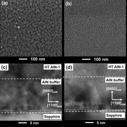
Figure 1. Surface morphologies of (a) MOCVD AlN buffer and (b) sputtered AlN buffer taken with scanning electron microscope (SEM) using magnification of 300,000. Cross-sectional high-resolution transmission electron microscope (HRTEM) images of (c) AlN film with MOCVD AlN buffer and (d) AlN film with sputtered AlN buffer.
The formation of nanoscale voids originates from the high-speed lateral growth and large depth/width ratio between three-dimensional islands. Similar to the case of epitaxial lateral overgrowth (ELOG), the pre-existing dislocations can bend and terminate at the local free surfaces provided by these voids, following the principle of dislocation line energy minimization. Because of a higher island density, the AlN film with sputtered AlN buffer has a higher void density of 1.7x1010cm-2 in the (0001) plane, providing a higher probability for dislocation termination. During the coalescence processes of the voids, the misorientations between the adjacent domains in the AlN film with sputtered AlN buffer are much smaller, so dislocations at the coalescence boundaries are also effectively suppressed.
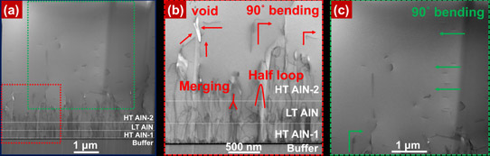
Figure 2: Cross-sectional dislocation distributions of AlN film with sputtered AlN buffer.
The 90˚ dislocation bending in the areas away from the voids is associated with macro-step movement. When the macro-step advances laterally and meets with the dislocation in the normal surface, the dislocation will bend as the macro-step and surface advance. The large ratio of lateral growth rate to vertical growth rate results in the 90˚ dislocation bending. The 90˚ bent dislocations propagate laterally. Therefore, it is easy for them to come into contact with other dislocations and block them by merging or forming half-loops.
Benefiting from this, only a few threading dislocations can reach the top surface of the AlN film with a sputtered AlN buffer. Plan-view transmission electron microscope (TEM) measurement shows that the TDD of the AlN film with the sputtered AlN buffer is dramatically reduced to an extremely low value of 4.7x107cm-2, which is 81.2% less than the TDD of the AlN film with an MOCVD AlN buffer.
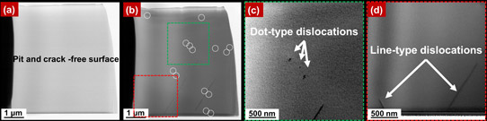
Figure 3. Plan-view TEM images of AlN film with sputtered AlN buffer.
Additionally, the 5.6μm-thick AlN film is crack-free and pit-free. The root mean square (RMS) roughness of the AlN film with sputtered AlN buffer is as small as 0.14nm over 3μm x 3μm. The concentrations of carbon, hydrogen, and oxygen are as low as 1.6x1017cm-3, 3.0x1017cm-3 and 1.3x1017cm-3, respectively.
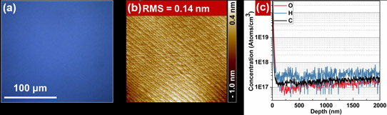
Figure 4. AlN film with sputtered AlN buffer demonstrates (a) crack-free and (b) atomically flat surface. (c) SIMS profiles of carbon, hydrogen and oxygen impurities.
The researchers say that the very simple yet effective technique demonstrates potential for the mass fabrication of low-cost and high-performance DUV devices.
https://pubs.acs.org/doi/10.1021/acs.cgd.8b01045


