


- News
6 November 2018
III-V heterojunction bipolar transistor MOCVD on 200mm (001) silicon
Researchers based in Singapore have used metal-organic chemical vapor deposition (MOCVD) to grow III-V heterojunction bipolar transistors (HBT) directly on 200mm-diameter silicon wafers [Wan Khai Loke et al, Semicond. Sci. Technol., vol33, p115011, 2018].
The team from Nanyang Technological University and Singapore MIT Alliance for Research and Technology (SMART) hopes that the technology could lead to integration with mainstream silicon complementary metal oxide semiconductor (CMOS) electronics using the most effective (001) crystal orientation.
The researchers foresee application in power amplifiers for mobile phone handsets. III-V HBTs have increased high-frequency performance compared with silicon-only devices. Further advantages can arise from bandgap tuning in terms of higher voltage breakdown and low-noise operation.
The researchers first grew a germanium buffer layer on a 200mm (001) p-type silicon substrate. The substrate was offcut 6° in the [110] direction. The epitaxial process was MOCVD of a thin silicon conditioning layer, followed by 60nm of 350°C germanium seeding and 740nm of a 650°C germanium buffer layer. The buffer was subjected to cyclic thermal annealing to control surface roughness to the order of 1nm and to reduce threading dislocation density to the 107/cm2 scale.
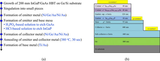
Figure 1: InGaP/GaAs HBT fabrication process flow (a), and schematic cross section of device (b).
The HBT structure was also grown by MOCVD, resulting in indium gallium arsenide phosphide (InGaAsP) alloys. Device fabrication used 2.54cmx2.54cm pieces diced from the 200mm epitaxial wafer (Figure 1). The emitter area was 40μmx50μm.
With 5V collector-emitter voltage, the DC gain of one device was 95. The ideality factors for the collector and base currents were 1.07 and 1.23, respectively. The base sheet resistance came in at 430Ω/square. The breakdown for collector-emitter, collector-base and emitter-base stresses were 9.35V, 13.2V and 9.69V, respectively.
In statistical studies over a number of devices, there was some variation of idealities (<6%) and breakdown (~9%, collector-base average 14.2V). The average gain of 73 varied around 28% - mainly due to variation of the base current. The researchers comment: “The variation of the base current could be due to the defect density, the thickness non-uniformity of the HBT device layers and the fabrication variation from sample to sample.”
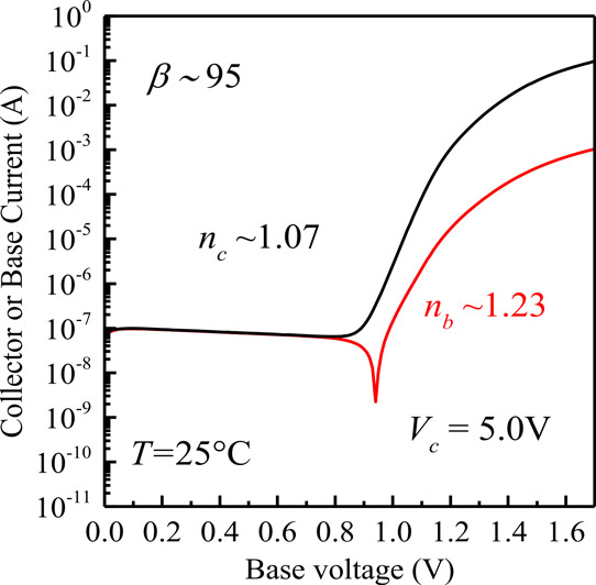
Figure 2: Gummel plot (25°C) of InGaP/GaAs HBT.
The researcher believe that, with optimization, the gain could be increased to 239.
https://doi.org/10.1088/1361-6641/aae247
The author Mike Cooke is a freelance technology journalist who has worked in the semiconductor and advanced technology sectors since 1997.


