


- News
7 November 2018
Lateral epitaxial overgrowth on silicon to boost ultraviolet output power
Researchers based in Japan, USA and Turkey have developed technology for high-brightness ultraviolet (UV) aluminium gallium nitride (AlGaN) light-emitting diodes (LEDs) using material grown on 200mm silicon substrates [Yoann Robin et al, Materials Science in Semiconductor Processing, vol90, p87, 2019]. The team from Nagoya University in Japan, Virginia Commonwealth University in the USA, Cumhuriyet University in Turkey and Northwestern University in the USA used lateral epitaxial overgrowth methods to improve material quality. The researchers report: “Improvement of the AlN quality and the structure design allowed the optical output power to reach the milliwatt range under pulsed current, exceeding the previously reported maximum efficiency.”
More efficient UV-emitting devices would improve the performance and cost effectiveness of laser printing, high-capacity data storage, white lighting, and water purification and sterilization. Growth on silicon, rather than much more expensive sapphire or silicon carbide, would reduce production costs. Also, silicon is available in larger-diameter formats for mass production. Another advantage of silicon is potential integration with smart driving circuitry based on mainstream CMOS electronics.
The drawback of growth on silicon is lower-quality material that reduces device efficiency. In particular, the epitaxial AlGaN layers are generally strained due to lattice-constant (~19%) and thermal expansion (~50%) mismatching with silicon.
The UV emitting material was grown on (111) silicon using metal-organic chemical vapor deposition (MOCVD). First a 120nm seed layer of AlN was grown and then patterned for lateral epitaxial overgrowth. The patterning consisted of 2μm-deep trenches along the [10-10] direction of the AlN structure ([[11-2] relative to silicon substrate). The trenching resulted in stripes that were 2μm wide with 4μm period.
Further AlN buffer growth was performed at high temperature with precursors delivered in hydrogen carrier gas in pulses. The growth of AlN on the seed stripes coalesced after about 6μm of growth. The AlN template was used as the base for the growth of 600nm of silicon-doped n-Al0.2Ga0.8N, five 3nm Al0.05Ga0.95N wells separated by 7nm Al0.15Ga0.85N barriers, a 10nm magnesium-doped p-Al0.3Ga0.7N electron-blocking layer, 100nm of magnesium-doped p-Al0.15Ga0.85N, and 50nm of magnesium-doped p-GaN. A comparison epitaxy of the same AlGaN structure was carried out on a 350nm AlN buffer on polished c-plane sapphire.
Fabrication of the LEDs began with rapid thermal annealing to activate the magnesium doping of the p-type layers. The 300μmx300μm device mesas were defined by electron cyclotron resonance (ECR) reactive ion etch. Nickel/gold and titanium/gold were deposited by electron-beam evaporation as the p- and n-type electrodes, respectively. Silicon dioxide was used for passivation. Further metalization added a thick titanium/gold layer that made contact with both electrode types.
The LED chips were flipped and mounted on pre-patterned AlN submounts with gold-tin eutectic bonding. The silicon substrate was removed using a hydrofluoric/nitric/acetic acid mix. The sides of the devices were protected with wax during the wet etching. Substrate removal is vital since silicon absorbs UV radiation, unlike sapphire. The devices were then bonded to copper heat-sinks with indium, and finally wire bonds were made for electrical connection. The comparison sapphire-based LED was fabricated similarly, but without substrate removal.
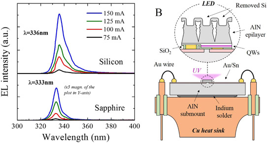
Figure 1: (A) Electroluminescence spectra of UV-LEDs grown on silicon and sapphire (Al2O3) recorded at different current densities. (B) Schematic of device structure grown on silicon.
The devices emitted a narrow peak around 336nm wavelength in 1%-duty-cycle pulsed operation (10μs period); the comparison LEDs grown on sapphire emitted nearby at 333nm (Figure 1). The full-width at half maximum (FWHM) of peaks were 8.9nm for material grown on silicon, compared with 6.6nm for sapphire-based structures. The performance of the devices were somewhat similar.
The UV-LED from silicon-grown material achieved a maximum output power of 1.3mW at 700mA injection with 0.5% duty cycle and 10μs period (Figure 2). Although this represents only a 0.13% wall-plug efficiency, the result represents one of the highest values reported so far for silicon substrate growth at this wavelength. At higher duty cycles the peak power reduced, most likely due to thermal effects related to Shockley-Read-Hall recombination. Moving to continuous wave (CW) operation reduces the peak power by a factor of 300. For the LED grown on sapphire, the corresponding reduction factor was just 10.
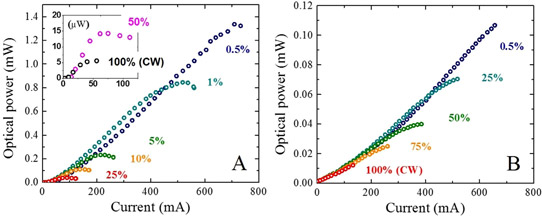
Figure 2: Optical output power measurements of UV-LEDs grown on silicon (A) and sapphire (B) as function of injection current for different duty cycles.
Near-field analysis under the microscope showed defective current spreading in the LED grown on silicon, unlike the sapphire-based device. The researchers found cracks on the AlN surface where the silicon substrate was removed. The team comments: “Further investigations indicated that few AlN cracks were visible right after the growth (non-coalesced area or thermal cracking for instance) and several ones were created during the device processing. Additionally, upon the substrate removal step, the acid mixture penetrated through the cracks and slightly etched the metal contacts and passivation layer of the LED/Si structure.”
Further damage was caused by localized regions of high current density leading to hot spots and thermal instability at higher currents and duty cycles. The researchers believes that these factors explain the greater reduction in peak power in moving to CW operation from UV-LEDs grown on silicon.
Lateral epitaxial overgrowth on silicon AlGaN LEDs Silicon substrates UV LEDs
https://doi.org/10.1016/j.mssp.2018.09.027
The author Mike Cooke is a freelance technology journalist who has worked in the semiconductor and advanced technology sectors since 1997.


