


- News
7 November 2018
Peking University provides evidence of substitutional C atoms occupying N site with −1 charge state in semi-insulating GaN
© Semiconductor Today Magazine / Juno PublishiPicture: Disco’s DAL7440 KABRA laser saw.
A team led by Peking University has provided what is said to be unambiguous evidence of substitutional carbon (C) atoms occupying the nitrogen (N) site with a −1 charge state in semi-insulating gallium nitride (GaN).
From the viewpoint of symmetry, it is demonstrated that the observed two local vibrational modes (LVMs) in the Fourier-transform infrared (FTIR) and Raman spectra originate from the substitutional C atoms occupying the N site with a −1 charge state. They are assigned to the non-degenerate A1 mode and the doubly degenerate E mode of C3v point group, respectively. This experimental data is said to be in excellent agreement with the calculated results [Shan Wu, et al, ‘Unambiguous Identification of Carbon Location on the N Site in Semi-insulating GaN’, Phys. Rev. Lett. 121, 145505 (2018)].
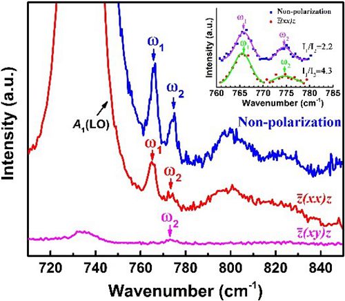
Figure 1 Room-temperature Raman spectra of heaviest C-doped GaN film in non-polarized, polarized configurations. Inset: enlarged fitting curves of LVMs.
Carbon doping is essential for producing semi-insulating GaN for fabricating high-electron-mobility transistors (HEMTs) and hence power electronics. However, despite C-related defects in GaN having been investigated for more than 20 years, it has has remained mysterious where carbon impurities reside in the GaN crystal lattice.
Now, the researchers at Peking University and their colleagues claim to have solved this long-standing problem through a combination of experimental and theoretical calculations, clarifying the lattice site of C in GaN using polarized FTIR and Raman spectroscopies in combination with first-principles calculations.
Two LVMs at 766cm-1 and 774cm-1 in C-doped GaN are observed. The 766cm-1 mode is assigned to the non-degenerate A1 mode vibrating along the c axis, whereas the 774cm-1 mode is ascribed to the doubly degenerate E mode confined in the plane perpendicular to the c-axis. The two LVMs are identified to originate from isolated with local C3v symmetry.
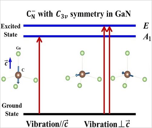
Figure 2 Schematic energy-level diagrams and fundamental dipole transitions in a center with C3v symmetry. Calculated vibrational directions of C atom are also depicted.
Experimental data and calculations are in outstanding agreement both for the positions and the intensity ratios of the LVMs. They are said to provide the first unambiguous evidence of the substitutional C atoms occupying the N site with a −1 charge state in semi-insulating GaN.
The researchers believe that the work will provide a universal approach for identifying the lattice sites of carbon in other compound semiconductors such as aluminium nitride (AlN), boron nitride (BN), zinc oxide (ZnO) and gallium oxide (Ga2O3).
https://journals.aps.org/prl/abstract/10.1103/PhysRevLett.121.145505


