


- News
28 November 2018
Gallium nitride microwire arrays on silicon for ultraviolet photodetection
South China Normal University and Peking University have developed ultraviolet (UV) metal-semiconductor-metal (MSM) detectors based on gallium nitride (GaN) microwire arrays on (100) silicon [Dexiao Guo et al, ACS Photonics, published online 1 November 2018]. The researchers claim superior performance compared with most reported GaN nano/microwire- or thin-film-based UV detectors. The team sees application potential for future photoelectronic and on-chip optoelectronic integrated systems.
The researchers used a top-down technique for creating horizontal microwires that should enable better repeatability in manufacturing compared with botton-up growth methods that suffer from random placement, and uneven diameter or curvatures, of vertical wires. Further, the technique avoids the need for complicated lift-off and layer transfer of structures to another substrate or other complex processes that increase production costs.
The 2-inch high-resistivity (100) silicon substrate was prepared with a 300nm plasma-enhanced chemical vapor deposition (PECVD) silicon dioxide layer that was patterned into 3μm stripes separated by 7μm silicon gaps. Potassium hydroxide wet etching of the silicon created trapezoidal channels with (111) facets that present a hexagonal atomic arrangement most conducive to III-nitride growth. Native oxide was then removed with hydrofluoric acid solution.
The microwire arrays were produced with low-pressure (100mbar) metal-organic chemical vapor deposition (MOCVD) of 300nm AlN insulating buffer and then unintentionally doped GaN (Figure 1). The wires were contacted with two patterned nickel/gold Schottky electrodes 20μm apart. Photoluminescence experiments showed a sharp and high-intensity near-band-edge emission peak centered at 364.5nm (~3.4 eV). Yellow luminescence, which indicates impurities and defects, was not observed.
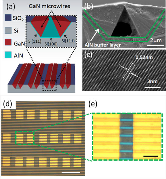
Figure 1: (a) Schematic of GaN-based microwire arrays on patterned silicon substrate. (b) Typical scanning electron microscope image. (c) High-resolution transmission electron microscope image of GaN microwire. (d) Optical microscope image of fabricated orderly arranged detectors; scale bar 100μm. (e) Enlarged image of one detector; scale bar 20μm.
With 5.0V bias under 2500μW/cm2 325nm helium-cadmium laser power, the current was 2.71mA. Dark current was 1.3μA, giving a sensitivity of 2.08x10⁵%. The current-light output power dependence followed a power law with exponent 0.995. The exponent being close to 1 indicates a low density of trap states and high crystal quality of the GaN microwires. The responsivity was calculated at 1.17x10⁵A/W, while the external quantum efficiency (EQE) came in at 4.47x10⁵. The maximum specific detectivity was 1016Jones.
The researchers claim that their UV photodetector performs in terms of high UV sensitivity, high responsivity and high EQE, much better than most reported single GaN nano/microwire- and nanowire-array-based photodetectors.
The team’s device also improves on most reported GaN-based alternatives in terms of a turn-on time of 36.3ms under 2500μW/cm2 illumination. During reset, there were two exponential processes – a fast one of 75.2ms, followed by a much more extended decay of 9.66s. The researchers suggest traps or other defect states could be involved in the persistent photoconductivity after turn-off of the light source. The researchers suggest that oxygen is desorbed from the surface during UV illumination. When reabsorbed the oxygen traps electrons, delaying the full return to the dark current state.
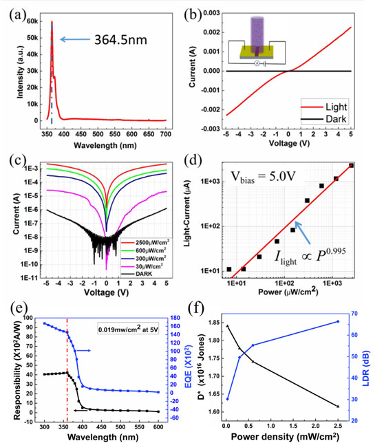
Figure 2: (a) Room-temperature micro-photoluminescence spectrum of GaN microwire; (b) current-voltage characteristics both in dark (black curve) and under 325nm UV illumination (red curve); inset, testing schematic diagram of photodetector; (c) light-density-dependent current-voltage curves; (d) current variation as function of light intensity; (e) responsivity and EQE-dependent wavelength curves; (f) specific detectivity dependent power density curves.
The team also created a comparison device on sapphire with 3μm GaN layer. The devices featured nickel/gold contacts. The electrode lithography used the same photomask as for the microwire device on silicon. The sensitivity, responsivity and EQE were 2.77x10⁴%, 0.21A/W and 0.80, respectively.
Ultraviolet metal-semiconductor-metal detectors GaN Silicon substrate GaN microwire arrays
https://pubs.acs.org/doi/10.1021/acsphotonics.8b00918
The author Mike Cooke is a freelance technology journalist who has worked in the semiconductor and advanced technology sectors since 1997.


