


- News
22 November 2018
Laser annealing enables gate-first fabrication of III-nitride transistors
South China University of Technology has used focused laser light to perform selective, micron-scale localized annealing of source and drain electrodes to enable gate-first fabrication of aluminium gallium nitride (AlGaN) high-electron-mobility transistors (HEMTs) [Zhikun Liu et al, IEEE Electron Device Letters, published online 23 October 2018].
Gate-first fabrication is standard in self-aligned silicon CMOS transistor fabrication. Adding gate-first GaN HEMT fabrication to the process palette could lead to novel integration options with Si CMOS such as creating new classes of digitally assisted RF mixed-signal and power conditioning circuits.
Typically, it would be preferred that the CMOS elements be processed before the AlGaN HEMTs. Unfortunately, thermal budgets of CMOS processing generally have an upper limit of 450°C to ensure that electrical performance is maintained. HEMT fabrication normally uses gate-last process flows because achieving ohmic contacts for source and drain electrodes needs very high temperatures of more than 800°C that would damage gate structures. These temperatures also clearly bust the thermal budget for silicon CMOS.
The HEMT structure consisted of a 20nm Al0.25Ga0.75N barrier layer on a 150nm GaN channel/buffer. The two-dimensional electron gas (2DEG) channel was formed near the GaN/AlGaN interface with 1.0x10¹³/cm2 carrier density, 1.5x103cm2/V-s mobility, and 450Ω/square sheet resistance.
The gate-first fabrication process flow began with plasma-enhanced chemical vapor deposition (PECVD) of 20nm of silicon dioxide. Electron-beam evaporation of nickel/gold gate metals was followed by patterning via lift-off lithography into 5μm-long, 600μm-wide gate structures. Patterned buffered oxide etching was used to remove the silicon dioxide insulation from the source/drain contact regions. Further electron-beam evaporation resulted in titanium/aluminium/nickel/gold source/drain electrodes. The source-gate and drain-gate spacings were 5μm and 10μm, respectively.
The annealing of the source/drain electrodes was achieved using 532nm continuous-wave laser light focused to a 3μm spot by a microscope objective lens. The aim was to thermally activate the out-diffusion of nitrogen from the AlGaN. The process was carried out in a home-made vacuum chamber at 5x10⁻³Pa pressure. Vacuum was critical for avoiding oxidation during annealing.
The laser spot scanned twice over the electrodes at 10μm/s speed. The laser power was between 0.84W and 0.96W for low-resistance contacts – the optimum was around 0.9W. Simulations suggested that the temperature at the center of the laser spot would be 850°C after 0.5s, while 6.5μm away the temperature would fall to 335°C.
Contact resistance as low as 0.3Ω-mm was achieved (2.2x10⁻⁶Ω-cm2 specific contact resistance). The researchers attribute the low contact resistance to the formation of a thicker ~35nm titanium nitride layer compared with the ~10nm of more conventional rapid thermal annealing (RTA). The thicker titanium nitride layer of the laser anneal is correlated with the formation of nitrogen vacancies in the underlying AlGaN, leading to the formation of an ohmic contact. Also, the fast temperature rise of ~2s allows nitrogen to escape through the titanium before titanium nitride crystallization at the interface.
Comparison gate-last devices were created with source/drain electrodes annealed rapidly at 850°C for 1 minute before reactive ion etching of the mesa and silicon dioxide deposition and gate formation. The contact resistance for this method was 0.8Ω-mm (7.2Ω-mm for 700°C annealing). Another effect of 850°C RTA was to increase the sheet resistance of the 2DEG to 600Ω/square, according to transmission-line method measurements. Further comparison devices were fabricated gate-first with lower-temperature RTA at 700°C and 800°C. The 800°C anneal destroyed the gate, while at 700°C the gate became defective, according to optical inspection.
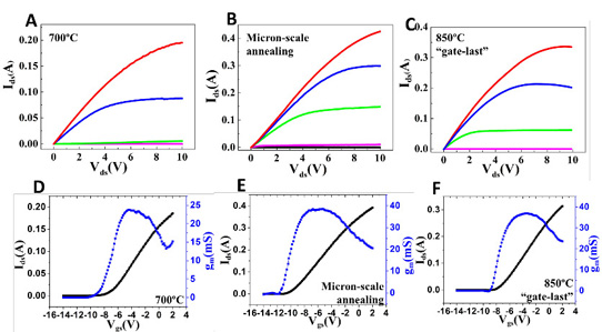
Figure 1: Output (A, B and C) and transfer characteristics (D, E and F) of devices processed by 700°C RTA , micron-scale annealing and gate-last approach, respectively.
The electrical performance of the gate-first micron-scale laser-annealed HEMTs showed higher drain current and transconductance compared with 700°C RTA gate-first and 850°C gate-last devices (Figure 1). With the gate at 2V, the maximum drain current for gate-first micron-scale annealing was 0.42A – 110% higher than for the 700° gate-first HEMT and 27% than the 850°C gate-last device.
The researchers point out that the profile of the transconductance laser-annealed device was flatter, suggesting better linearity and larger dynamic range in applications.
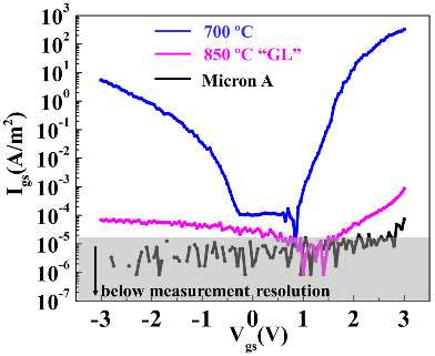
Figure 2: Gate current density-voltage (Igs-Vgs) characteristics of GaN MOSFETs processed by RTA at 700°C, micron-scale annealing and gate-last approaches.
Micron-scale annealing also limited gate leakage to less than 7x10⁻⁵A/m2 – comparable to the gate-last device and a factor of 106 lower than the gate-first 700°C HEMT (Figure 2).
Laser annealing AlGaN AlGaN HEMTs
https://doi.org/10.1109/LED.2018.2877717
The author Mike Cooke is a freelance technology journalist who has worked in the semiconductor and advanced technology sectors since 1997.


