


- News
4 October 2018
Black phosphorus photodiode for mid-wavelength infrared detection
Researchers based in the USA, Taiwan and Australia have improved the performance of mid-wavelength infrared (MWIR, 3-8μm) photodiodes using black phosphorus (bP) as absorbing material and a molybdenum disulfide (MoS2) electrode [James Bullock et al, Nature Photonics, published online 27 August 2018].
The team from University of California, Berkeley and Lawrence Berkeley National Laboratory in the USA, National Tsing Hua University in Taiwan and University of Melbourne in Australia claim that their devices can be competitive with conventional MWIR detectors. Further, the team used black phosphorus’ anisotropic optical response to “demonstrate the first bias-selectable polarization-resolved photodetector that operates without the need for external optics,” with the potential for astronomy, polarization-division multiplexing and remote sensing.
‘Van der Waals’ materials such as bP and MoS2 have many interesting properties due to their two-dimensional (2D) nature of strong in-plane but weaker between-plane bonds. The Van der Waals forces between planes avoid problems with ‘dangling bonds’ at the surface that can cause difficulties with devices based on conventional 3D bulk semiconductor materials. The 2D materials can be used to create thin absorbing layers with reduced noise from thermal electron-hole generation-recombination. Bulk semiconductor layers need to be thicker to reduce the effect of surface recombination at their problematic dangling bonds.
The bandgap of black phosphorus ranges from 1.5eV for monolayers shifting down to 0.3eV as the thickness increases, putting longer and longer wavelengths into the detectable range (~830nm out to ~4.1μm). At the same time, MoS2 is also a 2D Van der Waals material from the transition-metal dichalcogenide family.
The researchers are looking to MWIR applications in the medical, scientific, communication, automation and surveillance fields. They hope that the use of black phosphorus as absorber could overcome problems with other technologies such as expensive processing and the need for costly active cooling to reduce thermal noise.
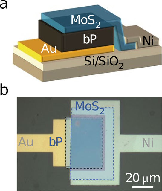
Figure 1: bP/MoS2 heterojunction photodiode concept. a, Schematic of device configuration, showing the heterojunction and contact configuration. b, Optical micrograph of a completed device; regions containing bP and MoS2 are outlined for clarity.
The devices consisted of a back pad/reflector of gold, black phosphorus, and a top window/contact of 10-20nm n-type MoS2 (Figure 1). The band offset between the black phosphorus and n-MoS2 enables electron flow into the contact material but blocks holes. The monolayer thicknesses of black phosphorus and MoS2 were 5.5Å and 6Å, respectively. Electron microscope analysis suggested some amorphous material at the bP/MoS2 interface, which was attributed to oxidation of the phosphorus due to air exposure during fabrication. The design of the device was optimized using simulations.
The optimum structure was expected to be 150nm black phosphorus and 15nm MoS2, giving a predicted ~80% absorption of polarized light at 3μm wavelength. The optimum polarization was along the ‘x’ or ‘armchair’ direction of the black phosphorus atomic structure (Figure 2). The moderately thin black phosphorus layer should reduce noise while still permitting high absorption in the narrow MWIR target spectral range.
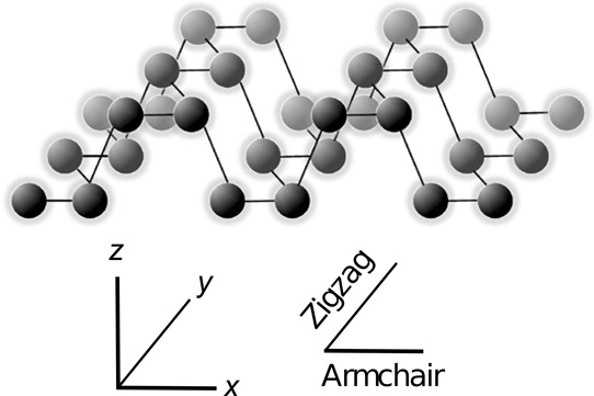
Figure 2: Schematic diagram of black phosphorus crystal structure.
A fabricated device demonstrated a peak external quantum efficiency (ηe) between 30% and 35% for radiation wavelengths between 2.5μm and 3.5μm (Figure 3). The researchers comment: “These are the highest ηe values reported for black phosphorus in this range at room temperature and correspond to current responsivity values of ~0.9AW-1.” Previous work has only managed ηe values less than 5% in the near-infrared and short-wavelength infrared regions.
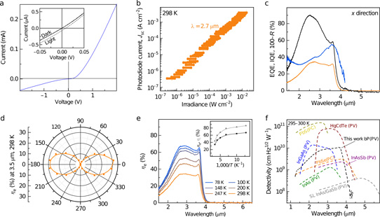
Figure 3: Photoresponse and detectivity characterization performed at zero bias. a, Current-voltage curve with inset measurements in dark and under illumination by 1000K blackbody source. b, Measured photocurrent as function of incident illumination intensity with2.7μm laser diode source. Error bars represent uncertainty in spot size. c, Spectrally dependent ηe , ηi and 100%-reflectivity (R). d, Variation of ηe with polarization angle at 3.5μm wavelength. e, Spectral ηe as function of temperature with inset ηe and ηi variation at 3μm. f, Specific detectivity versus wavelength at room temperature as well as various commercially available and reported MWIR photovoltaic (PV) and photoconductive (PC) detectors.
The device design targeted a quarter-wavelength interference peak at just below 3μm. The internal quantum efficiency (ηi) was estimated to be 40-50%. Moving the polarization of the incident radiation from the x to y (‘zig-zag’) directions reduced ηe from more than 30% down to less than 1%. Reducing the operating temperature to 78K increased ηe to 63% for 3μm infrared.
The detectivity (D*) peaked at 3.8μm with a value of 1.1x10¹⁰cmHz1/2/W, according to an estimate based on the zero-bias resistance area product. Unlike many more established technologies, the device was not biased to improve performance. A measurement based on noise equivalent power measurements under flood illumination from a blackbody source (from 100°C up to 400°C) gave a D* value of 7x10⁹cmHz1/2/W. The researchers consider the agreement between the two methods to be “good”.
The rise- and fall-time responses to 2.7μm infrared were 3.7μs and 4.0μs, respectively, “among the fastest reported for bP-based photoconductors and photodiodes,” according to the team. However, commercial devices have faster response, and the researchers hope that improvements could come from reducing the black phosphorus bulk trap concentration and eliminating defective interfacial layers with oxidant-free fabrication.
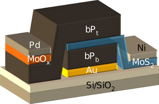
Figure 4: Polarization-resolved bP/MoS 2 heterojunction photodiode.
A more complex device was developed for polarization resolution. Two layers of black phosphorus with perpendicular crystal alignments were separated by a MoS2 electrode (Figure 4). The bottom black phosphorus had a gold contact, while the top black phosphorus layer used a stack of molybdenum oxide and palladium (MoOx/Pd) to collect holes. The arrangement allowed discrimination between radiation polarized in the two different directions.
https://doi.org/10.1038/s41566-018-0239-8
The author Mike Cooke is a freelance technology journalist who has worked in the semiconductor and advanced technology sectors since 1997.


