


- News
19 October 2018
High-performance light emission from III-nitride stress/dislocation control
Researchers in China have used stress and dislocation control measures to improve the performance of III-nitride on silicon light-emitting diode (LED) performance in terms of high output power and low forward voltage [Yuan Li et al, Journal of Alloys and Compounds, vol771, p1000, 2019]. Of course, such material can also serve as the basis for III-N electronics taking advantage of high voltage and high frequency handling capabilities. Growth on silicon reduces costs in terms of the material itself and from mass manufacturing on large-diameter substrates, compared with sapphire, silicon carbide and free-standing or bulk gallium nitride.
South China University of Technology and Guangdong Choicore Optoelectronics Co Ltd in China prepared the (111) 4-inch silicon substrates by 1100°C thermal cleaning and native oxide removal in the metal-organic chemical vapor deposition (MOCVD) reaction chamber. The first layer was a 250nm aluminium nitride (AlN) nucleation buffer grown at 1150°C. The transition to gallium nitride (GaN) was enabled by a range of aluminium gallium nitride (AlGaN) transition buffers (Figure 1).
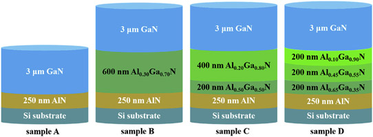
Figure 1: Structures of GaN epitaxial films for samples A, B, C and D.
The materials from samples ‘B’ and ‘C’ were used to create LED structures with the following layer sequence: 500nm of undoped GaN, 3μm of n-GaN, 9x(3nm/12nm) of InGaN/GaN quantum wells, a 20nm AlInGaN electron-blocking layer, and 200nm of p-GaN. Samples B and C were chosen since they were crack-free, unlike samples A and D. X-ray analysis suggested higher crystal quality of the cracked wafers as a result of stress release, but such substrates are unsuitable for device epitaxy and fabrication.
The LEDs were fabricated in a vertical format with the growth substrate removed below the 3μm n-GaN layer, and top and bottom metal contacts applied to the p-GaN and exposed n-GaN layers, respectively.
The cracks in samples A and D were attributed to the 56% mismatch in the coefficient of thermal expansion and consequent stress build up from cooling from the growth temperature to ambient room conditions. The researchers note that, while the improved GaN buffer layer structure results from step-graded AlGaN transition layers, “the cracks on the surface of sample D show that the compensation effect may become weaker with the further increase in the number of AlGaN layers and the further decrease in the Al composition of top buffer layer.”
Raman spectroscopy gave estimates for the residual stress in samples A-D, in alphabetical order, of 0.37GPa, -0.05GPa, 0.39GPa, and 0.41GPa.
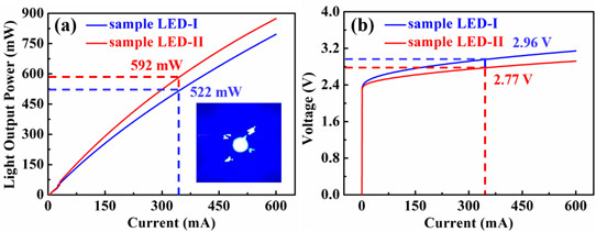
Figure 2: (a) Light output power versus current, and (b) voltage versus current curves from vertical structure LED chips of samples LED-I and LED-II, and photograph of lit-up LED chips working at 350mA inserted in (a).
The average light output power at 350mA for the LEDs on samples B and C were 522mW (LED-I) and 592mW (LED-II), respectively (Figure 2). The corresponding operating voltages were 2.96V and 2.77V. The electroluminescence wavelength peak was at 456nm.
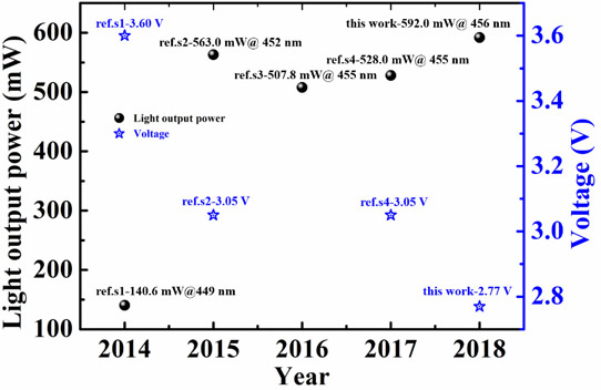
Figure 3: Properties of state-of-the-art high-power LEDs on silicon substrates working at a current of 350mA.
The higher output power and lower operating voltage of LED-II indicates higher efficiency as a result of higher crystal quality and smoother surface morphology. The vertical diode structure enables higher performance compared with state-of-the-art GaN grown on silicon LEDs through improved current spreading in the thick n-GaN layer (Figure 3).
LEDs GaN AlGaN AlN MOCVD Silicon substrates
https://doi.org/10.1016/j.jallcom.2018.09.031
The author Mike Cooke is a freelance technology journalist who has worked in the semiconductor and advanced technology sectors since 1997.


