


- News
10 October 2018
Argon-ion-enhanced room-temperature bonding with low resistance
A research team based in Japan and China has been developing room-temperature bonding enabled by argon ion exposure of gallium arsenide (GaAs) and silicon (Si) along with gallium arsenide and gallium nitride (GaN) [Yoshiaki Ajima et al, Appl. Phys. Express, vol11, p106501, 2018].
The scientists from Chiba Institute of Technology in Japan and Suzhou Institute of Nano-tech and Nano-bionics (SINANO) in China were particularly keen to produce bonds with low resistance. The GaN//GaAs bond achieved an interface resistance of 2.7Ω-cm2 - “the first reported instance of a bonded GaN//GaAs wafer with a low electrical resistance,” according to the researchers.
The team sees applications for “artificial photosynthesis”, using III-V materials to generate hydrogen and oxygen, while decomposing carbon dioxide. The decomposition of greenhouse gases and generation of energy-rich molecules has obvious economic and environmental benefits. Panasonic has demonstrated the use of GaN/pn-SI and InGaN/pn-Si multi-junction structures with potassium bicarbonate electrolyte, giving almost 1% solar energy conversion efficiency, much higher than the 0.2% of biological photosynthesis. The GaN or InGaN materials were not bonded to the pn-Si, but rather there was an airgap and the connection was via wires.
The Chiba/SINANO group hopes that their low-resistance bonded materials could help towards better efficiency. In particular, the room-temperature process avoids problems from thermal expansion mismatches between the materials. At the same time, bonding rather than epitaxial processing also avoids the defects introduced by lattice-constant mismatching.
Direct bonding of p-GaAs with n-Si was first compared with bonding through sputtered indium tin oxide (ITO) interlayers on both samples. The surfaces of the directly bonded samples were prepared with alkaline and hydrochloric acid cleaning processes. The metal contacts for electrical testing were applied before bonding: unannealed titanium/platinum/gold for the p-GaAs, and annealed titanium/platinum/silver for the n-Si.
Also, the researchers bonded n-GaN with p-GaAs. The p-GaAs had the same preparation and metal electrodes as above. The n-GaN had an annealed titanium/aluminium electrode.
The bonding was carried out in a chamber from Mitsubishi Heavy Industries Machine Tool capable of containing vacuums less than 10-5Pa. The room-temperature bonding was enabled with exposure to argon ions with kinetic energies in the range 60-80eV and a bonding force of 20MPa.
The directly bonded p-GaAs//n-Si junction exhibited an ohmic-like current-voltage (I-V) characteristic, in contrast with the Schottky junction behavior of the p-GaAs/ITO//ITO/n-Si bond (Figure 1).
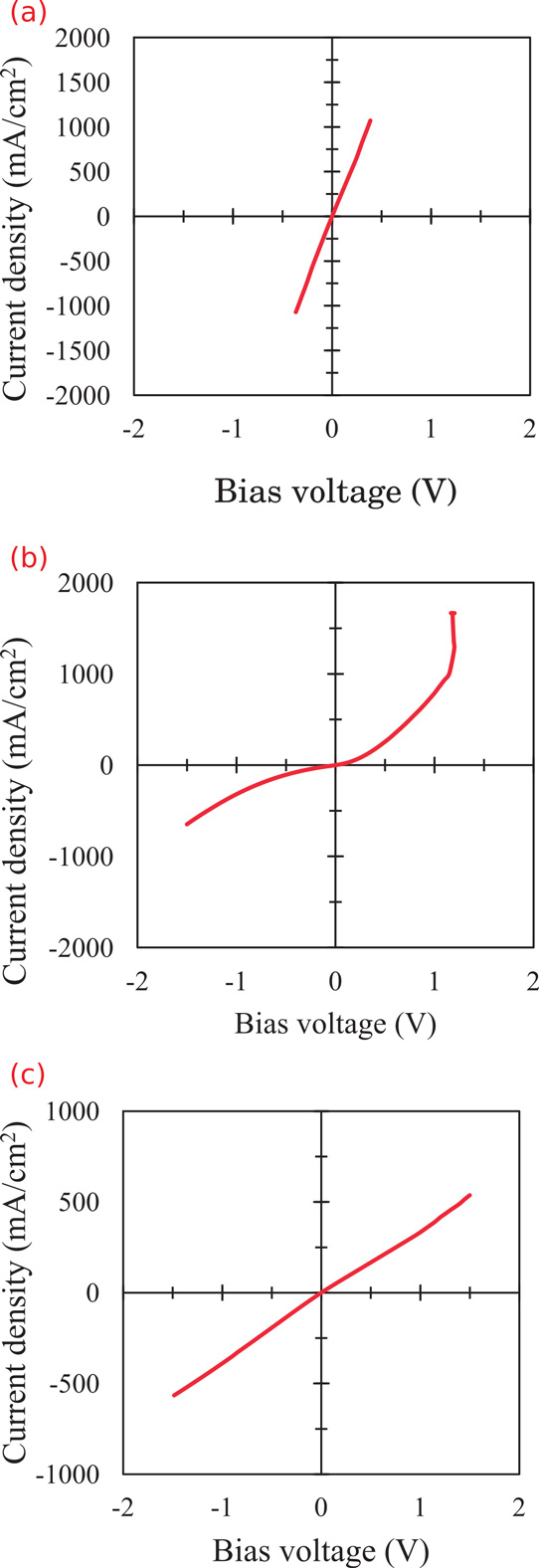
Figure 1: Current-voltage characteristics of (a) p-GaAs//n-Si; (b) p-GaAs/ITO//ITO/n-Si; and (c) p-GaAs//n-GaN bonded materials.
The interface resistance of the p-GaAs//n-Si sample was estimated to be 0.32Ω-cm2. Although a lower 0.079Ω-cm2 resistance has been achieved with bonding of n-GaAs on ITO/p-Si (n-GaAs//ITO/Si), the structure is seen as being unsuitable for photovoltaic applications due to the refractive index difference between ITO and silicon leading to the reflection of incoming radiation, reducing the absorption of light in silicon subcells.
The team comments: “The interface resistance for the p-GaAs//n-Si sample without ITO was low enough for the unit to operate under relatively low irradiation conditions, ranging from 1 to 5 suns. Furthermore, this configuration should reduce the degree of interface light reflection.”
The n-GaN//p-GaAs bonded interface also demonstrated an ohmic behavior with a resistance of 2.7Ω-cm2. The researchers claim this to be “the first report of a conductive GaN//GaAs bond with linear I–V characteristics”.
The researchers also investigated the high resistance of n-GaN//p-GaAs relative to the p-GaAs//n-Si bond. They found increased levels of iron and chromium from the chamber walls incorporated into the interface, as detected by energy-dispersive x-ray (EDX) analysis. This was attributed to the low-energy argon ion treatment. Iron doping is used to create semi-insulating GaN. There was also an increased oxygen EDX signal, presumably due to surface oxidation.
Transmission electron microscopy (TEM) revealed a 2-5nm amorphous layer between the materials. The high resistance, it is suggested, is due to the large difference in bandgap between GaN (3.39eV) and Si (1.42eV). Using narrower-bandgap InGaN as an interlayer could reduce the interface resistance, the team believes.
https://doi.org/10.7567/APEX.11.106501
The author Mike Cooke is a freelance technology journalist who has worked in the semiconductor and advanced technology sectors since 1997.


