


- News
6 September 2018
Activating buried p-type gallium nitride for power electronics
Cornell University, IQE RF LLC and Qorvo Inc in the USA have been working out ways to better activate buried p-type layers of gallium nitride (p-GaN) [Wenshen Li et al, Appl. Phys. Lett., vol113, p062105, p2018]. In most GaN/III-N growth processes the p-type layers are left until last because of the difficulty of activation, which usually involves heating the sample in an attempt to drive out hydrogen that passivates the magnesium doping used to create mobile hole charge carriers.
This p-GaN-last constraint limits the sort of structures that can be explored for power electronics and other applications. Examples of buried-structure devices include heterojunction bipolar transistors (HBTs), trench metal-oxide-semiconductor field-effect transistors (MOSFETs), current-aperture vertical electron transistors (CAVETs), and laterally diffused MOSFETs (LDMOSFETs).
The team used the reverse breakdown measurements for assessing p-GaN activation as “a sensitive probe pertinent to power electronic applications”.
Metal-organic chemical vapor deposition (MOCVD) produced epitaxial layers on bulk GaN (Figure 1). The top p-GaN layers were activated in-situ. The researchers report that the contact resistance (~4x10⁻⁵Ω-cm2) and Hall measurement (hole density ~7% magnesium concentration, mobility 24cm2/V-s) results for this material with a top p-GaN layer were “among the best in the literature”.
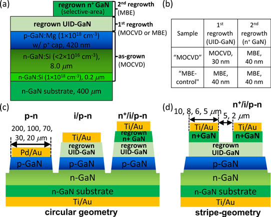
Figure 1: (a) Schematic layer structure of as-grown in-situ activated p-n diode structure and two re-grown layers. (b) Information on two re-grown layers on MOCVD and MBE control samples. (c) Schematic cross sections of three types of circular diode: p-n, i/p-n and n+/i/p-n diodes fabricated on both samples. (d) Schematic cross section of n+/i/p-n diodes with stripe geometry. Stripes all have a finger length of 50μm.
The p-GaN was then buried using re-growth via blanket MOCVD or molecular beam epitaxy (MBE) of undoped GaN. For the MOCVD sample, the p-GaN was passivated with 900°C annealing in ammonia for 30 minutes in the reaction chamber. The MOCVD sample was also prepared by ultraviolet-ozone and hydrofluoric acid treatments to reduce silicon residues. For the MBE sample, the buried p-GaN was unpassivated. A final n+-GaN layer was grown selectively by MBE on the two samples.
The material was used to create a series of buried p-GaN structures for electrical testing with contacts using various stacks of palladium (Pd), titanium (Ti) and gold (Au). Various dry etch recipes were used to remove the undoped GaN re-grown top layer and for mesa isolation. The buried p-GaN was activated by annealing at 725°C for 30 minutes in dry air, driving hydrogen out through the mesa sidewalls. The metal contacts were applied after annealing.
Probing unmetalized MOCVD-sample structures without buried p-GaN activation showed high leakage currents under reverse bias. The leakage was suppressed by activation.
The reverse-bias breakdown occurred in the range 1100-1200V for annealed circular p-n and i/p-n diodes, independent of diameter (Figure 2). Breakdown damage was observed as a burnt region at the mesa edge, typical for devices without field plates or other edge termination structure. The researchers estimate more than 28% activation of the magnesium acceptors in the p-GaN layers, as calculated from the field distribution at punch-through. The team sees this as a lower bound on activation as “breakdown is limited by edge field crowding but not punch through”.
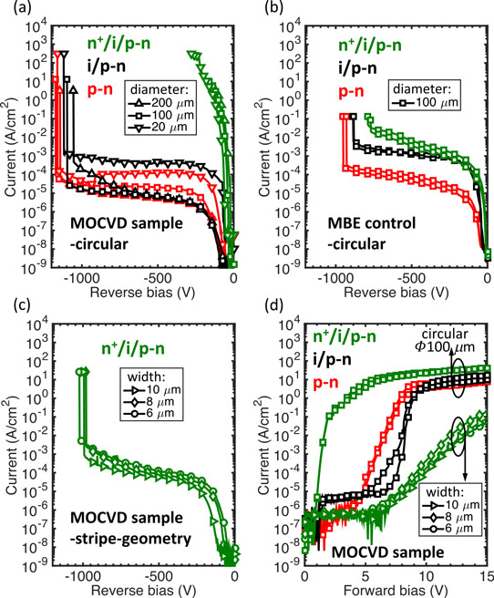
Figure 2: Reverse and forward current density versus voltage characteristics of diodes. (a) Reverse-bias characteristics of circular diodes on MOCVD and (b) on MBE control samples. (c) Reverse-bias characteristics of n+/i/p-n diodes with stripe geometry on MOCVD sample. (d) Forward-bias characteristics of various diodes on MOCVD sample.
The n+/i/p-n-diodes had much higher leakage, and current-dependent soft breakdown occurred at 300V. MBE-sample devices had much lower leakage, attributed to the absence of hydrogen in the re-growth.
The high leakage in n+/i/p-n diodes is attributed to the n+-GaN layer blocking the diffusion of hydrogen out of the buried p-GaN layers. For the i/p-n devices, magnesium diffusion into the undoped (UID) GaN cap converts it into a p-GaN layer, allowing hydrogen diffusion upward during activation. Even with 20μm-diameter circular devices, diffusion of hydrogen through the mesa sidewalls is not sufficient for effective p-GaN activation.
Narrower-stripe-geometry devices with widths between 10μm and 5μm reduced the leakage current and enable breakdown to reach comparable values to the circular p-n and i/p-n diodes. The researchers comment: “These data indicate sufficient activation of the buried p-GaN, and thus a lateral hydrogen diffusion length of >5μm (half of the stripe width) under the annealing conditions used in this work. The observed activation should be attributed to the lateral diffusion of hydrogen out of the etched mesa sidewall as well as the exposed UID-GaN surface between fingers.”
The forward bias characteristics of the p-n and i/p-n circular devices are similar – the turn-on voltage is rather high, and the on-current low, due to poor ohmic contact with p-type GaN.
The n+/i/p-n devices were back-to-back diodes and hence should not have a high current in the ‘forward’ bias region. The high current of the circular n+/i/p-n diodes demonstrates high leakage and hence poor p-GaN activation. By contrast, the leakage is suppressed in the stripe devices.
The researchers see 10-20μm as the critical lateral dimension range for effective activation of buried p-GaN through annealing. This range allows the escape of hydrogen out of p-GaN surfaces with a diffusion length of 5-10μm.
The researchers comment: “The reverse breakdown measurement is a much stricter test of the acceptor activation of buried p-GaN than light emission. Any insufficient activation of buried p-GaN leads to drastically higher leakage current due to premature punch-through.”
The team also suggests that activation of magnesium near the surface creates an electric field that attracts hydrogen ions (mainly protons), enhancing out-diffusion. However, the effect of concentration gradient and electric field is reduced when the lateral dimension through which the hydrogen is required to diffuse increases.
IQE RF p-GaN MOSFETs MOCVD CAVETs
https://doi.org/10.1063/1.5041879
The author Mike Cooke is a freelance technology journalist who has worked in the semiconductor and advanced technology sectors since 1997.


