


- News
21 September 2018
Vertical-cavity resonant near-green lasing of indium gallium nitride
Xiamen University and Suzhou Institute of Nano-Tech and Nano-Bionics (SINANO) in China have developed near-green vertical-cavity surface-emitting lasers (VCSELs) using material that is mainly luminescent in the blue 445nm part of the spectrum [Rongbin Xu et al, IEEE Transactions on Electron Devices, published online 3 September 2018].
The researchers engineered the cavity resonance so that it favored the near-green 493nm-wavelength emissions from indium gallium nitride (InGaN). Efficient green laser diodes are highly desired to plug the ‘green gap’ for red-green-blue full-color display systems. Presently, green laser light is produced using a combination of a longer-wavelength laser and frequency-doubling, increasing complexity, system sizes, and cost.
Researchers are seeking to plug the gap with InGaN-based devices, but the material suffers from inhomogeneous composition and crystal quality degradation, especially at the higher indium contents needed for green emission.
The active region consisted of a double quantum well of In0.18Ga0.82N, 2.5nm each, separated by 6nm of GaN. Normally such material is expected to emit blue wavelengths around 445nm. The wells were capped with an electron-blocking layer of 20nm of Al0.2Ga0.8N to prevent carrier overflow into the p-type layers. The metal-organic chemical vapor deposition (MOCVD) of III-nitride material was performed on c-plane sapphire.
The epitaxial material was fabricated into a VCSEL (Figure 1) with distributed Bragg reflector (DBR) mirrors defining the cavity and a silicon dioxide (SiO2) current aperture. The DBRs used titanium oxide (Ti3O5) and silicon dioxide dielectric pairs – 13.5 for the bottom mirror and 11.5 for the top. Indium tin oxide (ITO, 30nm) was used for current spreading in the aperture. The p- and n-electrodes were both chromium/gold (Cr/Au). The structure was flipped onto a copper (Cu) heatsink.
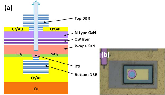
Figure 1: (a) Cross-sectional schematic of VCSEL. (b) Optical image of real device.
At a low 15mA current, the emission centers on the ~440nm blue range of the InGaN quantum well material (Figure 2). As the current increases to the 32mA (~18kA/cm2) threshold, the wavelengths in the cavity resonance region of 493nm become stronger, based on emissions from In-rich localized narrow-gap regions. At higher 45mA current injection, the ~440nm wavelengths are suppressed and a narrow lasing peak emerges with 0.55nm linewidth in the blue-green 493nm region. The output power at 50mA was estimated to be ~178μW. Previously, the researchers report that they produced quantum dot VCSELs in the green region, but with only 10μW light output power. The optical polarization of the emitted light was 71% at 1.09x the threshold current injection.
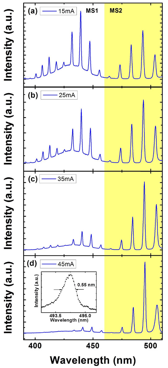
Figure 2: Electroluminescence spectra of the VCSEL measured at four different currents. (a) 15mA, (b) 25mA, (c) 35mA, and (d) 45mA. Inset: linewidth of lasing peak measured with higher resolution.
The cavity resonance compensates for the lower density of In-rich localized narrow-gap regions, reducing the lifetime for recombination into photons. The researchers comment: “The short lifetime indicates a high carrier capture efficiency and can compensate the low density of emission centers, resulting in stronger emission intensity.”
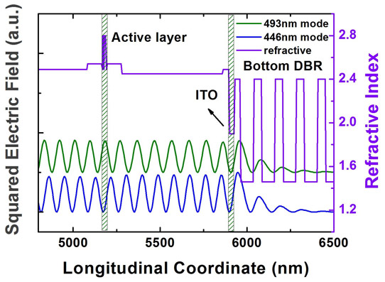
Figure 3: Refractive index and distribution of optical field for 446nm and 493nm cavity modes of VCSEL.
Simulations of the optical field also suggest that the active region lines up with an anti-node (maximum) of the standing-wave pattern for 493nm wavelength emissions. By contrast, the 446nm mode gives a node (minimum) at the active layers. The gain enhancement factor is calculated at 1.82 for 493nm and 0.21 for 446nm. The researcher also point out that the longer lasing wavelength also benefits less absorption loss in the active region.
https://doi.org/10.1109/TED.2018.2866406
The author Mike Cooke is a freelance technology journalist who has worked in the semiconductor and advanced technology sectors since 1997.


